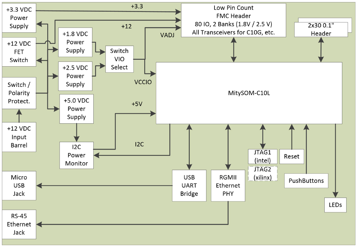
MitySOM-C10L Development Kit Architecture
Block Diagram

Key Elements of the Development Kit
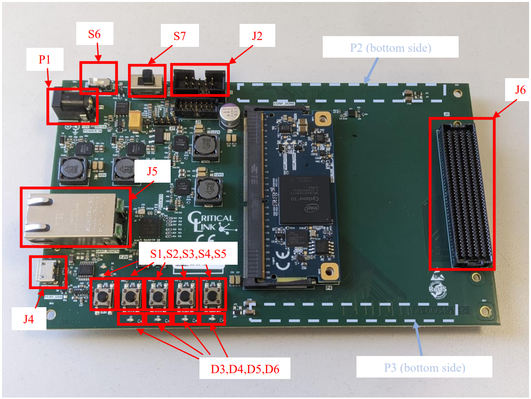
An annotated photo of the Development Kit, with SOM Module inserted, is shown below. It shows the location of all connectors, switches and LEDs required for use of the Development Kit and for demonstrating the operation of the SOM Module itself using the MitySOM-C10L Reference Design or custom user design.

A list of the highlighted Development Board items follows.
| Reference Designator(s) |
Description |
|---|---|
| P1 | 12V Input Power Connector |
| S6 | Main Power switch to Development Kit |
| S7 | Vccio Voltage Select: 1.8V/2.5V controls all 3 SOM Vccio rails: Vccio_23, Vccio_45 and Vccio_68 |
| J2 | JTAG Header for USB Blaster |
| J4 | Micro-USB connection for USB-UART |
| J5 | RJ-45 Ethernet connector |
| J6 | FMC Header (LPC connections only) FPGA I/O |
| P2 & P3 | Expansion I/O Headers (on bottom side) |
| S1 | nCONFIG: Start FPGA Reconfiguration |
| S2, S3, S4 & S5 | User Pushbutton Inputs (to FPGA I/O) |
| D3, D4, D5 & D6 | User Indicator LEDs (from FPGA I/O) |
Go to top

