MityDSP-L138 Architecture
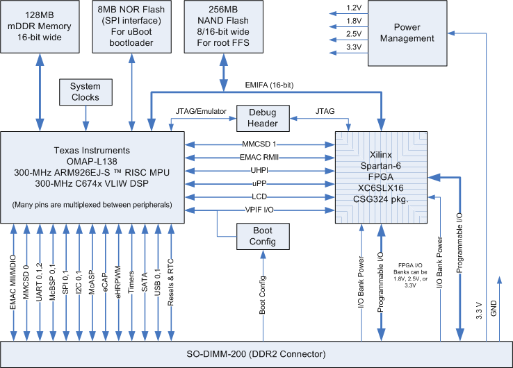
The top level block diagram of the MityDSP-L138 module is illustrated in the figure below. It is possible to upgrade the FPGA, NAND FLASH, and DDR RAM capacities upon customer request. NOTE this figure indicates 300 MHz core clock speed. It should be updated as the MityOMAP-L138 architecture supports 375 MHz. There is also an option for a 450 MHz clock speed configuration.

Non-Volatile Storage
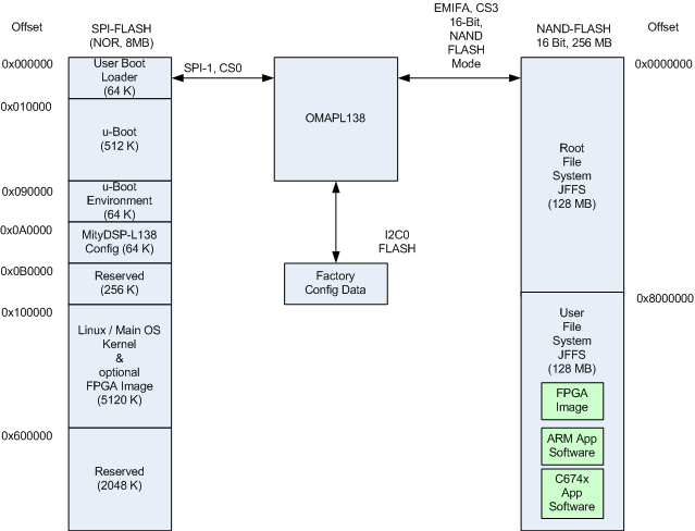
The factory non-volatile storage for the MityDSP-L138 and MityARM-L138 modules is shown in the figure below. This figure represents only those modules located in the SOM itself. The SOM includes an 8 MByte SPI-NOR flash, and a 256 MByte NAND flash. Additional storage on the main carrier card (MMC FLASH, Compact FLASH, SATA, etc.) of a specific application is not shown.

Boot Process
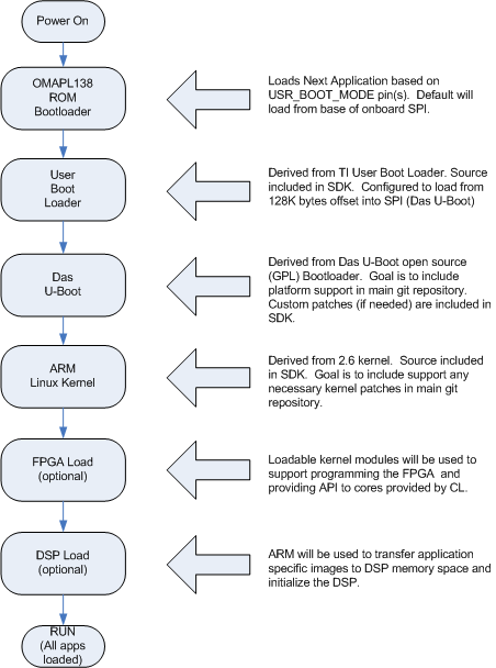
The figure below illustrates a typical boot sequence for a MityDSP-L138 running Linux on the ARM and an optional DSP and FPGA image.

Details for the boot sequence are described in the list below.
1. On power-up or reset, the OMAPL138 ROM based bootloader is executed. Based on the boot select pin on the MityOMAP edge connector, the CPU will load a TI AIS bootscript image into the ARM from either the on-board SPI-1 NOR Flash (default) or off of UART1. The factory provided SPI-NOR image is the ARM CPU User Boot Loader Image, and is loaded into the ARM internal memory. Source code for the UBL is available for the MityDSP under the GPL license. The TI AIS bootscript also allows for configuring the external memory interface registers as well as the PLL settings prior to launching the loaded program.
2. Once loaded, execution is transferred to the UBL. This program essentially loads u-Boot (also in SPIproper-1 NOR Flash) into mDDR2, but also allows modification to the various CPU low level settings including the PLL's, DDR configuration, and pin multiplexing configuration that may be necessary to get u-Boot loaded and running.
3. u-Boot is the third stage bootloader that is executed out of external DDR2 memory. u-Boot will configure the serial ports, ethernet ports, and optionally the MMC interface and will provide the low level user interface for updating the on-board FLASH memories. The u-Boot port by Critical Link also supports loading the FPGA (for modules including an FPGA) if it must be loaded prior to launching the operating system load. Note: typical updates (user application loads, etc.) can happen after the MityDSP-L138 or MityARM-1808 ARM has completely loaded up and started the linux kernel.
4. u-Boot is configured at factory to allow the user to break into it (via console keystroke) within 3 seconds. If no user interaction is detected, it will load into the ARM the linux kernel image and start the linux operating system. The location of the linux kernel and the root filesystem is application specific. User's may elect to store the kernel and root filesystem on the on-board SPI-NOR, on-board NAND, an attached MMC controller, an attach SATA hard disk, or on an NFS server. USB stick is also supported, but has not been tested or verified at Critical Link.
5. Once the operating system has booted, access to several non-volatile storage filesystems is available. User applications for the ARM, as well as DSP applications (for the OMAP-L138 variant SoMs) can be launched via startup scripts at runtime. In addition, for modules with FPGAs, FPGA device drivers can be loaded to support FPGA configuration and control.
Go to top

