On-SOM Clocks
The MitySOM-A5E includes 2 main clock sources as shown in the figure below.
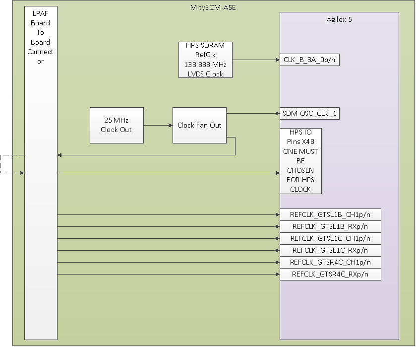
The first clock source is specifically intended for the HPS EMIF LPDDR4 clocking. It is a 133.33333 MHz LVDS clock that is run into the Bank 3B clock inputs and used as a reference clock for the LPDDR PLL configuraiton.
The second clock source is 25 MHz, which is buffered to provide 2 outputs. 1 output is fed directly into the FPGA Secure Data Manager (SDM) OSC_CLK_1 port. The second output is routed to the samtech interface pins. The intent is to allow the user to loop this clock signal back to the FPGA HPS IO pin that will be used to clock the HPS. The HPS can use any HPS GPIO pin as the reference clock pin, and the design decision to route the reference clock to the baseboard was made in order to allow flexibility in the hardware design of the carrier cards in order to maximize the HPS IO options available to the designer.
As shown in the figure, several of the transceiver reference clocks have been routed from the FPGA to the baseboard connector in order to support various clocking schemes for the transceiver lanes.