MitySOM-C10L FPGA Reference Design
- Table of contents
- MitySOM-C10L FPGA Reference Design
Reference Design Summary
The MitySOM-C10L FPGA Reference Design provides a convenient starting point for custom designs and for understanding the capabilities and interfaces of the MitySOM-C10L and Development Kit products. It includes example interfaces to all on-SOM hardware (clock, LEDs and memory devices) as well as to Development Kit baseboard devices (LEDs, switches, UART, I2C bus) and expansion I/O headers. A block diagram of the reference design is shown below:

As can be seen in the above diagram, the reference design is built around a Nios II soft processor Platform Designer system, with several interface IP cores (including optional interfaces shown in dashed lines & shaded light orange).
SLL HyperRAM Memory
If you are planning to use the SLL HyperRAM Memory, please visit xSPI Memory Controller IP to request a download for the IP to use in the design. Once the IP is obtained, it can be extracted into the ip folder such as mitysom-c10l-ref/C10L-7Q-3X3-RI_HyperRAM/ip/20230420_SLL-CL_MBMC-v3_2_15-RD-24hr-NIC (Note: SLL IP name subject to change). The SLL HyperRAM Memory is only available for the 80 KLE FPGA SOM variant.
Reference Design Download
The Reference Design and related documentation can be downloaded via Critical Link's Git Repo here: MitySOM-C10L Reference Design
The git command line to fetch the reference design repository, from under Linux or within a Nios II Command Shell in Windows, is shown below:
user@linux # git clone git://support.criticallink.com/home/git/mitysom-c10l-ref -b mainThe Reference Design includes a Makefile and all required source files to create:
- An Intel Quartus Prime Project
- VHDL design source file(s)
- Intel Platform Designer (formerly QSYS) subsystem(s)
- Reference Nios-II SW Project (Application and BSP)
- A basic console application accessible via USB-UART
- App can test and exercise most SOM hardware and interfaces to the baseboard
- Top-level pin constraints,
- Also included is an Excel Spreadsheet to assist in creating pin constraints for custom designs
- Basic timing constraints
Execute Quartus Project Makefile
After all prerequisites have been met, proceed to start the Nios II Command Shell and change the working directory to the desired subdirectory for your SOM variant and application use under the location that you had cloned/downloaded the reference design project to. Below is a description of the subdirectories and their application use.
- C10L-7N-3XX-RI
- For use with the 16 KLE FPGA SOM variant.
- C10L-7Q-3X3-RI
- For use with the 80 KLE FPGA SOM variant.
- C10L-7Q-3X3-RI_HyperRAM
- For use with the 80 KLE FPGA SOM variant and the SLL HyperRAM Memory IP.
- C10L-7Q-3X3-RI_LWIP
- For use with the 80 KLE FPGA SOM variant. The SLL HyperRAM Memory IP is mandatory for this project directory. See LWIP_IP_Stack_Example_Design for more information.
So, assuming you have a kit with the C10L-7Q-3X3-RI (80 KLE FPGA) and would like to use the SLL HyperRAM Memory IP, you will change to the C10L-7Q-3X3-RI_HyperRAM directory
Once in the desired project directory, you will see a Makefile provided for use. Run the command make all to build the NIOS and generate the SOF & JIC file for the SOM. For a list of available targets for the Makefile and more information, run the command make help.
If the Makefile generates error messages or fails in any way, please visit the #Troubleshooting section below.
Interface Limitations on some SOM Models
Some MitySOM-C10L Modules have more limited hardware resources available, both in terms of the FPGA sizing itself (fewer Logic Elements and internal RAM Blocks) as well as having no external HyperRAM device installed. The Makefile is aware of these limitations and will either warn the user of certain optional selections that are likely to cause errors while compiling the pre-made reference design or prevent automatic insertion of larger design blocks (such as the Ethernet subsystem). Please heed these warnings during the initial project setup, which is meant to demonstrate the capabilities of the MitySOM-C10L.
The C10L-7N-3XX-RI in particular has a small, 16 KLE Cyclone 10 LP FPGA (10CL016Y) and does not include the HyperRAM option on board. The limited resources on this SOM make it unrealistic to have an Ethernet interface (both the HW and SW requirements for this are too great for the 10CL016Y FPGA).
Once the reference design project is created (and optionally compiled), the user may customize the project in any way that will fit within the limitations of the selected FPGA (size and speed grade). A fully custom design, including one not based upon a Nios-II MCU Platform Design at all, can also be constructed from scratch, using the reference design and documentation (such as the Pin Constraint Excel Spreadsheet) as a guide for the successful design and use of the SOM in your own system.
Reference Design Directory Structure
Once the reference design is setup/built, you will see the following directory structure. Note, this example follows the C10L-7Q-3X3-RI_HyperRAM project.
.
├── README.md
├── docs
│    └── MitySOM-C10L_GoldenRef_Pinout.xlsm
│
├── C10L-7N-3XX-RI             # MitySOM-C10L 16 KLE FPGA Project Directory
├── C10L-7Q-3X3-RI             # MitySOM-C10L 80 KLE FPGA Project Directory
├── C10L-7Q-3X3-RI_LWIP             # MitySOM-C10L 80 KLE FPGA Project Directory with LWIP IP Stack Examples
│
└── C10L-7Q-3X3-RI_HyperRAM             # MitySOM-C10L 80 KLE FPGA Project Directory with SLL HyperRAM Memory
     │   # Reference Design Makefile:
     ├── Makefile
     │
     │   # Several helper Tcl scripts called by the Makefile, Do NOT modify these:
     ├── bsp_boilerplate_commands.tcl
     ├── create_dev_c10l_ref_quartus.tcl
     ├── ...
     ├── gen_reference_bsp.tcl
     │
     │   # Sources used by scripts to create the Project:
     ├── mitysom_c10l_ref_top.vhd.terp
     │
     │   # Design Constraints:
     ├── mitysom_c10l_ref_top.sdc
     ├── rgmii.sdc
     │
     │   # Generated Files:
     ├── mitysom_c10l_ref.jic       # QSPI NOR FLASH Programming File (converted, combined output of HW and SW builds)
     ├── mitysom_c10l_ref.qpf       # Intel Quartus Project File
     ├── mitysom_c10l_ref.qsf       # Intel Quartus Settings File (FPGA design settings, including pin constraints)
     ├── mitysom_c10l_ref_top.vhd   # Top-level VHDL Design file
     ├── nios_sys.qsys              # Platform Designer file for Nios-II CPU subsystem
     ├── nios_sys.sopcinfo          # SOPCINFO file required in the generation of the BSP
     ├── rgmii_eth_subsystem.qsys   # (Optional) Platform Designer file for Ethernet subsystem
     │
     ├── ...                        # Other directories and files generated by Quartus tools
     └── software
          ├── mitysom_c10l_ref
          │     ├── mitysom_c10l_ref.c    # Primary C Source file for Console Application
          │     ├── ...                   # Other C source and Header files
          │     │
          │     ├── Makefile              # Makefile for building the BSP and SW application
          │     ├── mitysom_c10l_ref.elf  # ELF for built application
          │     │
          │     ├── obj                   # Compiled object files
          │     └── mem_init              # Memory Initialization Files (used for FLASH Programming file generation)
          │            ├── intel_generic_sfi.hex
          │            └── ...
          │
          └── mitysom_c10l_ref_bsp        # Generated Board Support Package project files (includes HAL and drivers)
Programming the SOM
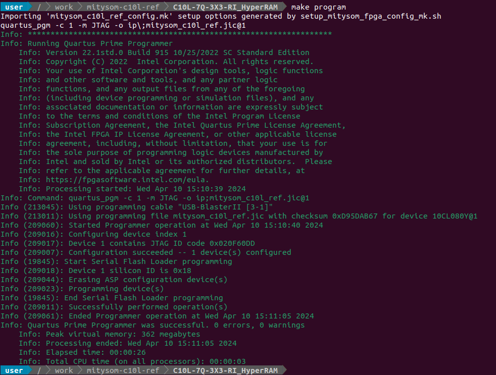
After the Makefile finishes building the reference design FPGA HW, compiles the application SW and creates the FLASH Programming File (.JIC), you can program the SOM's FLASH with either the Quartus GUI tools or by running the command make program.
Note that this will erase and overwrite the Factory Default FPGA configuration in the SOM's FLASH. Ensure that power is on and that the USB Blaster JTAG programmer is properly connected to the Development Kit in J2 before proceeding. Upon successful FLASH programming, you should see:
After successful programming, you should either power-cycle the Development Kit using slider switch S6 or force a reconfiguration of the FPGA from FLASH by depressing the nCONFIG pushbutton switch S1.
If the FLASH programming is unsuccessful, please:- Check power and USB Blaster connections to the board (for reference, see MitySOM-C10L Development Kit Architecture),
- Ensure that the JIC file was created without error, or
- Contact Critical Link for additional assistance.
- Check to make sure the FPGA correctly configures itself from FLASH by verifying that both the CONF_DONE and PWR_GOOD LEDs on the SOM are illuminated,
- If not, please contact Critical Link
- If you have made Hardware or Software changes to the Reference Design, please review your changes and double check that the pin constraints are valid (you can also verify the final compiled FPGA pinout inside the Quartus GUI using either the Pin Planner or by reviewing the pinout report file),
- Other troubleshooting steps: TODO
Restoring to Factory Default
In order to reprogram the SOM's FLASH with the factory default version of the reference design for your SOM, perform these steps:
- Within the project subdirectory, run the command make scrub_clean which will restore the design to its barebones state.
- Run the command make default_config
- Rebuild the Nios and recreate the SOF and JIC file using the command make all
- Reprogram the SOM's FLASH device using the steps outlined above in #Programming the SOM (i.e. type make program from within the project directory).
Running the Reference SW Console Application
The MitySOM-C10L Development Kits are delivered with the Reference Design (HW and SW) pre-programmed into the SOMs configuration FLASH. So, the following instructions apply whether you are testing your kit for the first time or if you used the Makefile to setup/build the reference design and programmed the FLASH yourself.
Th Reference SW application is a console application that provides status and control of the Reference Design over the USB-UART (J4 on the Development Kit baseboard). Use a terminal emulator program with settings: 115200 bps, 8/N/1. At power-up, or upon reconfiguration of the FPGA (e.g. by pushing switch S1 on the baseboard), in addition to the SOM & baseboard LEDs cycling through a pattern (indicating the reference design has loaded correctly), you should see some FPGA build information and SOM Factory Configuration data displayed on the console, like this:

As indicated in the console, you can see a full list of supported commands by typing help:

Note: more information about each command and syntax can be displayed using the help command's verbose switch (help -v).
The console application has a few U-Boot-inspired commands, like md and mw, in addition to several commands that highlight operation of SOM Module and baseboard features (iictest, ledtest and IOxxx commands) and a few utility commands (reset, info, etc.).
Memory access commands
The Memory Dump/Write commands (md and mw) provide a direct method of peaking and poking the Nios-II memory and IP core register locations. You can view the full Nios system memory map by opening the nios_sys.qsys in Platform Designer (from within Quartus Prime with the mitysom_c10l_ref project open). The Memory Map will look something like this, depending on which setup/build options you enable:

Detailed register memory maps for each individual Intel IP core can be found in the documentation associated with the IP core itself. The documentation is generally found by accessing the Details tab for an IP core from within Platform Designer. Many of the IP are covered here: Embedded Peripherals IP User Guide but some cores (like the Triple-Speed Ethernet Intel FPGA IP), have their own dedicated User Guide, so it is best to check the Details tab for the IP itself.
IO Read/Write/Config commands
The optional FMC header (J6) and Expansion header (P2 & P3) interfaces are connected to several PIO (Parallel I/O) Intel FPGA IP cores in the Nios system Platform Design. Each of these interfaces have a few header pins connected to Input-Only pins on the Cyclone 10 LP FPGA, while the rest of the pins are Input/Output/Bidir capable. When enabling the FMC and/or Expansion I/O interfaces in the reference design Makefile, it requires 3 PIO Intel FPGA IP cores for each interface (each core is limited to 32 signals) to handle all of the bidirectional I/O on each of these interfaces. Note: the Input-only pins are all mapped through a common PIO Intel FPGA IP core configured to be input-only (PIO_INPUTS).
The console IOxxx commands provide the ability to:- Read the current state of all input values on these Expansion I/O headers (using ioread),
- The state of the Dev Kit baseboard Pushbutton switches S2 - S5 (mapped to core BUTTONS_PIO, bits 0-3) are also displayed with the ioread command
- Set the direction of bidirectional I/O pins (using ioconfig <PIO Core #> <Direction Value>) where '0' sets the pin as an input, '1' as an output, and
- Set the output value for pins defined to be outputs with the ioconfig command above (using iowrite <PIO Core #> <Output Value>)
Note that the ioread command does not require any parameters (like the ioconfig or iowrite commands) but will simply read the input states for all enabled modules and display in the console.
The FMC Header I/O includes:- 4 Input-only pins (CLK0_M2C_P/N and CLK1_M2C_P/N), mapped to PIO_INPUTS[19:16]
- 68 Bidirectional pins, mapped to FMC_IO_0[31:0], FMC_IO_1[31:0] and FMC_IO_2[3:0]
- 8 Input-only pins (EXT1_CLK0_P/N, EXT1_CLK1_P/N, EXT2_CLK0_P/N and EXT2_CLK1_P/N), mapped to PIO_INPUTS[7:0]
- 84 Bidirectional pins, mapped to EXPANSION_IO_0[31:0], EXPANSION_IO_0[31:0] and EXPANSION_IO_2[19:0]
For reference, the PIO Core mapping for FMC & P2/P3 headers is provided below (for use with the iowrite and ioconfig commands):
| Console Coresel Value | PIO Core Name | PIO Bits | Connector Pin Name |
|---|---|---|---|
| 1 | FMC_IO_0 | 0-31 | LA00_P/N - LA15_P/N |
| 2 | FMC_IO_1 | 0-31 | LA16_P/N - LA31_P/N |
| 3 | FMC_IO_2 | 0-3 | LA32_P/N - LA33_P/N |
| 4 | EXPANSION_IO_0 | 0-31 | EXT1_DIO1_P/N - EXT1_DIO11_P/N, EXT1_DIO23 - EXT1_DIO32 |
| 5 | EXPANSION_IO_1 | 0-31 | EXT1_DIO33 - EXT1_DIO42, EXT2_DIO1_P/N - EXT2_DIO11_P/N |
| 6 | EXPANSION_IO_2 | 0-19 | EXT2_DIO23 - EXT2_DIO42 |
Note: the EXT1... signal names are mapped to the P2 header and the EXT2... signals go to the P3 Header.
Refer to the Reference Design pin constraints, the MitySOM-C10L_GoldenRef_Pinout.xlsm spreadsheet, or MitySOM-C10L Gen 1 Dev Board DataSheet [pdf] for the full list of pin numbers.
Customizing the Design
Once you have used the Makefile to create the FPGA project (and optionally compile the FPGA), you can open the project from within the Intel Quartus Prime software GUI (v22.1 Standard or later is recommended) and view/edit design sources, project settings and compilation results. The project can also simply be used as a starting point for creating your own custom design with the required interfaces to your own custom hardware baseboard and system. Finally, you can manually build the FPGA from within the GUI after making any changes to HW or SW elements of the project. The sections below will give a brief overview of the MitySOM-C10L Reference Design in the Quartus software environment. Instructions on how to use the Intel Quartus tools is outside the scope of this Wiki. However, tutorials, software user guides for the Quartus software tools and more assistance can be found at:- Getting Started: Introduction to the Quartus GUI
- Intel Quartus Software Introduction: YouTube Video
- Intel FPGA YouTube Channel: https://www.youtube.com/@IntelFPGA
- Full set of Quartus Prime Standard User Guides: Quartus Prime Pro and Standard Software User Guides
- Other Quartus Software Documentation: Intel Quartus Standard Documentation
- Intel FPGA Training Resources: Intel FPGA Technical Training
- Intel FPGA Support: Intel FPGA Support Resources
MitySOM-C10L FPGA Reference Hardware
After the Makefile has run successfully, you should see the Quartus Project file mitysom_c10l_ref.qpf in the fpga subdirectory (as shown in #Reference Design Directory Structure). Start the Intel Quartus Prime software and open this project file from within the Quartus GUI. Note: It is recommended that you open the project from within the GUI itself, especially if you have multiple versions of the Quartus software installed on your computer (to ensure that the project is opened in the correct version of the software). If you only have one version installed, you could also just double-click on the *.qpf file to open it in Quartus.
Once opened, if you expand the design hierarchy (in the Project Navigator pane in the upper-left portion of the GUI window) you will see the top-level VHDL design file at the top of the list (mitysom_c10l_ref_top) which can be viewed by double-clicking on it & you will see something like this:

Perusing this file, you will also see the primary design component, nios_sys (a Nios II based Platform Design), declared and instantiated in the top-level VHDL along with some logic and mapping of all I/O of the internal system to the FPGA top-level signal names (mapped to physical FPGA pins in the FPGA constraints and settings described further below in #FPGA Pin Constraints and other Project Settings).

You can now open the nios_sys subsystem in Platform Designer (formerly known as QSYS) by double-clicking on nios_sys in this same Project Navigator pane with the design hierarchy expanded. Note: The full design hierarchy is only visible if you had enabled the FPGA compilation process when running the reference design Makefile or you have manually compiled the design. If not, you will only see the top-level VHDL file listed there, so you will have to open the nios_sys using a different method such as by starting Platform Designer from within the GUI using either the toolbar button or in the Quartus Menu under Tools -> Platform Designer. You should now see something like this (with clock domain highlighting turned on):

Note: The IP available in your nios_sys Platform Design may be different, depending on which optional Interfaces were enabled when you ran the Makefile.
The Main System Contents Tab in the center of this window shows the Nios II processor, on-chip RAM, PLL and all I/O IP elements along with their interconnections to each other and exported interfaces (to the top-level VHDL file you had just looked at). In order to tailor this reference design to your own needs, you can add, delete or modify settings and/or connections for any of the IP in the existing Platform Design. Notice the IP Catalog pane (left side of this window) which provides a catalog of other available IP cores available to the user for insertion into this design.
Double-clicking on any IP in the current Platform Design will open a new tab called Parameters showing all settings for the core that you can modify. Also note the Details button near the top-right of the Parameters tab ... clicking this will take you to links to documentation and other information available for this IP element.

While navigating the nios_sys design, if you have chosen to enable the Ethernet PHY interface when running the Makefile, you may notice the rgmii_eth_subsystem is present but does not have any parameters shown in the Parameters tab. This design entity is actually another Platform Designer subsystem (rgmii_eth_subsystem.qsys). The Platform Designer tool supports hierarchical system designs and you can drill into this subsystem to view/edit the design the comprises this subsystem. You can drill into the lower-level subsystem by either using the hierarchy navigation buttons (near the top of the System Contents window tab) or by right-clicking on the name of the subsystem and selecting Drill into subsystem from the pop-up menu:

Note that any changes to the design, either in rgmii_eth_subsystem or nios_sys that requires interface changes (interfaces need to be Exported to the top-level VHDL) will also require regeneration of the Platform Design, modifications to the top-level VHDL and a recompilation of the entire FPGA Hardware. For assistance with any of these steps, please use the Quartus help system or visit the links provided above in #Customizing the Design.
After any changes to the FPGA Reference Hardware Design (or creating your own custom hardware design), you will need to compile the FPGA design in the Quartus GUI and ensure that no errors occur. This will generate an SOF-format programming file that can either be programmed into the FPGA directly using JTAG, or converted into the JIC-format FLASH programming file (along with any SW HEX images built below) for writing to the non-volatile FLASH configuration device on the SOM. Once the FLASH has been programmed, the MitySOM-C10L will boot from FLASH automatically on power-up (or when the nCONFIG pushbutton switch S1 on the Development Kit baseboard is pressed).
FPGA Pin Constraints and other Project Settings
All Pin constraints (location and I/O standards) as well as Quartus settings for the FPGA project are saved in Quartus Settings File (mitysom_c10l_ref.qsf file created by the Makefile). You can edit these manually using a text editor (however, it is best to close the Quartus software first or ensure that the Quartus Project is not open while editing this file), or use the appropriate window or dialog box listed under the Assignments Menu in the Quartus GUI:

We have also included an Excel Spreadsheet (MitySOM-C10L_GoldenRef_Pinout.xlsm under the docs directory) in the reference design repository to assist the user in creating pin constraints for your own custom design. This spreadsheet has embedded macros (Microsoft Excel will typically disable macros by default for security purposes - you will have to enable these to use this functionality). A quick view of the Macro button controls within this spreadsheet follows:

We have separated the FPGA Pin constraints into On-SOM Connections (fixed functionality, do not change these) and SOM Edge Connector connections (all I/O which is routed to the Development Kit baseboard or your own custom baseboard). You will notice a spreadsheet Tab for each of these pin types, as well as a 3rd Tab with the Reference Design default connections SOM Edge Connector - Dev Board.
To use this spreadsheet effectively, you would enter custom signal names and I/O standards you require into the Baseboard Signal Name and I/O Standard columns of the spreadsheet for the appropriate connections (note the Edge Connector Pin # columns). After doing this for all connections that your design requires, hitting the Generate Pin Constraints button will write out settings to a Tcl file (pin_constraints.tcl).
The Macro button controls are described below:
- Generate Pin Constraints: Writes all Som Edge Connector signal names and I/O standards to a Tcl file,
- Clear Signal Names & Standards: Deletes all assignments on this tab, to start from a clean slate,
- Cope Dev Board Names & Stds: Copies all Reference Design Signal Names and I/O Standards from the SOM Edge Connector - Dev Board tab to the SOM Edge Connector tab, and
- Import Constraints from file: will import existing constraints (from a .tcl, .qsf or .sdc format file) and populate the ones that match the FPGA pin numbers on the SOM Edge Connector tab.
Once all pin constraints are entered and you've generated the Tcl file(s), you can either copy all of the Tcl commands into your FPGA Project's QSF File (again, ensure that the project is not open in Quartus at the time) or simply source the Tcl files from within the QSF file (and removing existing pin constraints).
MitySOM-C10L FPGA Reference Software
Since the HW reference design is built around a Nios-II processor, we have also provided a simple console-based software application (described above in #Running the Reference SW Console Application) to exercise and highlight the operation of many of the interfaces present in the MitySOM-C10L Development Kit (LEDs, switches, I2C devices, FLASH, GPIO, etc.). This reference SW can be used as a starting point in the development of custom Nios SW for your own product built upon the MitySOM-C10L.
For complete information on the development of software for the Nios and instructions on how to use the Eclipse-based Nios II Software Build Tools (SBT), please see: Nios II Software Developer Handbook
Note: The current reference SW application does not exercise or use the HyperRAM device at this time. A separate, 3rd party IP core to interface to the HyperRAM is available through Synaptics Laboratories Ltd. The user may obtain the IP and license directly through them or develop your own logic to interface to the HyperRAM device. Also, the current version of the Nios-II Reference Software does not provide networking functionality at this time but may be added at a future date.
The software Board Support Package (BSP) and application is created and compiled by the Makefile if you have enabled compilation of the FPGA HW and generation of the SW and FLASH programming files. The setup process performs the necessary steps to compile the application using the command-line build tools. However, it does not automatically generate an Eclipse workspace and C Projects for the BSP and application for use with the Nios Software Build Tools GUI (Eclipse-based) which was installed when you installed the Intel Quartus Prime software along with the other steps listed above in the prerequisites.
You can either view/modify the software source files using any text editor and run the command-line tools yourself to regenerate the BSP & application executable, or you can follow the steps below to import the BSP and application into an Eclipse workspace to view, modify and or build the application in the Eclipsed-based flow.
Steps to Import BSP and Application


Steps to Create Custom Application


Steps to Build Application and Generate Memory Initialization files


Steps to Generate the FLASH programming file


Notes about the Reference Software Run Environment
The MitySOM-C10L Reference Design software application is configured to execute directly from FLASH, as opposed to running from within the FPGA On-chip RAM (OCRAM). In part, this has to do with the limited OCRAM available for Nios Software Instruction and Data memory. This is especially true in the smaller 16 KLE FPGA model of the SOM, which has about 56 Kbytes total (56 M9K RAM blocks) of available CPU storage, some of which is currently dedicated for Instruction and Data Caches ... reducing the available memory even more. For comparison, there is 16 Mbytes of FLASH non-volatile memory available on the SOM. SOM models with a HyperRAM device available on them will also have access to up to 32 Mbytes of volatile memory available for use through the SLL interface IP, which opens the door to more robust software applications with an RTOS and possibly even a networking stack. The Reference SW application, while relatively simple does require more instruction and data space as-is than what is available in the smallest FPGA version of the MitySOM-C10L.
Therefore, the Reference SW application is configured to run out of FLASH (the .text linker section is placed there), whereas the FPGA OCRAM is used for data storage, stack & heap space. This is important to be aware of, especially when creating your own custom HW design and/or SW application to run on the MitySOM-C10L product.
The flow steps described above (from HW design, through Custom SW application development, to the FLASH programming file creation) are written with the assumption that the code will run out of FLASH. However, if you need to run directly out of FPGA OCRAM instead and your application code/data requirements will fit in the OCRAM available, then you will have to modify the build steps accordingly. Running from FLASH is convenient for the purpose of the included console application reference SW, however it does complicate the debug process (especially when developing new SW from scratch) where it is more desirable to run out of OCRAM instead.
Note that in order to run from OCRAM instead of FLASH, changes will be required in several elements of the Reference Design HW and SW such as:- Nios II hardware parameters should be changed to ensure that both the Reset Vector and Exception Vector are in OCRAM,
- BSP Configuration changes:
- Linker sections should all be placed in OCRAM,
- hal.linker options for the bootloader, under Advanced settings in the BSP Editor may need to be changed
- A different HEX file output (from the SW application build and memory initialization file generation steps) will be required
- Instead of using the intel_generic_sfi.hex added as a HEX Data block in the FLASH programming file generation, you will likely need to use the cpu_ram.hex file while generating the FPGA Hardware SOF file instead, also requiring changes to the settings when creating the FLASH programming file itself (COF settings).
- Nios II Software Developer Handbook
- Nios II Processor Reference Guide
- Quartus Prime Manual: Programmer and Convert Programming Files Utility User Guide
- An Intel Nios II Example design flow booting from FLASH: GSFI and Nios II booting Quick Start Guide
Troubleshooting
Here are some details and solutions to potential errors that may occur while running the MitySOM-C10L Reference Design Makefile.
Makefile Failure while building Reference SW
Typical Error Messages
make[1]: nios2-elf-gcc.exe: Command not found
or:
Error (17923): Can't save or open file ./software/mitysom_c10l_ref/mem_init/intel_generic_sfi.hex
or:
Error: FLASH Programming file creation Failed!

and scrolling up in the command shell window, you can see the root cause of the error:

- OS = Windows 11, with WSL v2
- Intel Quartus Prime Standard 22.1, Build 915
It appears that this configuration setup (possibly others), that the Nios II Command Shell does not setup the PATH environment variable correctly in order to find the gcc cross-compiler executables. Inspecting the PATH environmental variable within the Nios Command Shell, you may notice that the Nios Command Shell has incorrectly appended the following directory:
/mnt/c/intelFPGA/22.1std/nios2eds/bin/gnu/H-i686-pc-linux-gnu/bin
which does not exist in the Windows 11 OS installation of Quartus. The correct directory should be:
<Install Directory>/nios2eds/bin/gnu/H-x86_64-mingw32/bin, or /mnt/c/intelFPGA/22.1std/nios2eds/bin/gnu/H-x86_64-mingw32/bin in the default installation directory location. The problem seems to stem from the fact that the Nios Command Shell is running under WSL and appears to be a Linux environment, so the wrong location is appended to the PATH.
Try one of these steps:
- Manually add the correct directory to your PATH environment variable. This should be done within the Nios Command Shell itself, which is running in a Linux (WSL) environment. This could be done by adding to the PATH in the user .bashrc file, or other method of your choosing. This would provide the correct PATH variable automatically the next time you start the Nios Command Shell (actually both locations will be now in the PATH, one of which is invalid).
- Not recommended - but you could force the correct PATH location be added (instead conditional assignment of the PATH based on the environment) by manually editing the <Install Directory>/nios2eds/nios2_command_shell.sh. Note: You can only do this if you have administrative privileges on the computer.
Go to top

