SoM pinout verification
Added by Mark Hamilton about 11 years ago
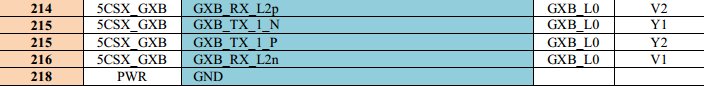
Parsing the datasheet prior to establishing a carrier board design, I observed the following flaw:
The table on pg 18 of the SoM datasheet available on the wiki (dated 19 November 2014) has pin 215 listed twice and omits pin 217.
From context and schematic print of development kit carrier, it seems clear that the topmost table entry for GXB_TX_1_N signal is actually pin 217 and my operating assumption is the rest of the data related to these two pins is accurate with this substitution.
Please let me know if this assumption is invalid.
| MityPins.png (17.8 KB) MityPins.png | Screengrab of datasheet segment indicated |
Replies (2)
RE: SoM pinout verification - Added by Adam Dziedzic about 11 years ago
Thank you for the info - we will correct the details.
Your assumption is correct. Additional design guidelines can be found on the MitySOM-5CSx Wiki:
https://support.criticallink.com/redmine/projects/mityarm-5cs/wiki/Wiki
With lots of information in the Carrier Board Design Guide (See p.20 for the edge connector interface schematic):
http://www.criticallink.com/wp-content/uploads/MitySOM-5CSX-Carrier-Board-Design-Guide.pdf
RE: SoM pinout verification - Added by Mark Hamilton about 11 years ago
Thanks Adam. I'd been floating through the wiki and referencing the design guide heavily as well.
Follow up on this comment, there are definitely other aspects of the table in the SoM datasheet indicated that are not in line with the schematic/design guide, notably pin mapping on banks 3A/5A.
I had initially based my mapping efforts around the datasheet table given ease of parsing, but have since rebased from the design guide which clearly better represents the board at this time.

