MityDSP-L138F Block Diagram Inconsistencies
Added by Dylan Louviaux almost 2 years ago
All,
I am designing a carrier board for the MityDSP-L138F with A7 FPGA. I have noticed some inconsistencies with the block diagrams in the documentation (https://www.criticallink.com/wp-content/uploads/2014/01/MityDSP-L138F_Spec.pdf).
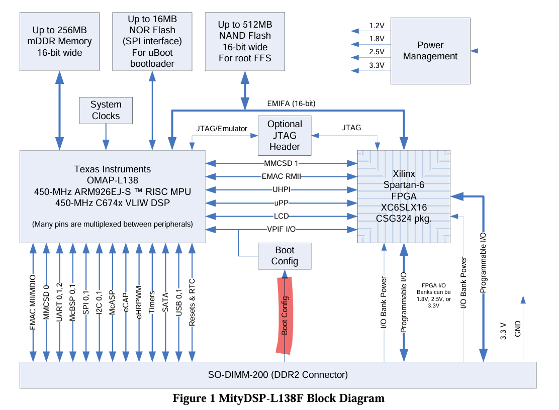
My issue is with the Boot Config block. The diagram indicates that there are inputs from the 200 pin connector to the VPIF/uPP/LCD bus with a "Boot config" block in-between. I cannot find any intuitive pin descriptions on the 200 pin connector on the MityDSP-L138F data sheet that describe any of the three pin functions on Table 1 in the docs. This issue extends to the TI OMAP-L138 documentation (https://www.ti.com/lit/ds/symlink/omap-l138.pdf?ts=1718026916499&ref_url=https%253A%252F%252Fwww.ti.com%252Fproduct%252FOMAP-L138) as I cannot find any of those interfaces on table 1 in the CL docs either. This leads me to believe there is no external input to this boot config block from the 200 and Id like to know more about the boot config block as a whole.
clipboard-202407191205-bumil.png
Replies (2)
RE: MityDSP-L138F Block Diagram Inconsistencies - Added by Daniel Vincelette almost 2 years ago
Hi Dylan,
The external input to the Boot Config Block is the EXT_BOOT# signal pin bin 12 of the SO-DIMM connector. The Boot Config Block on the SOM uses the value of EXT_BOOT# to set the boot strap resistors for the L138. The two options are booting are as follows:- EXT_BOOT# is high or floating(it's pulled up on the SOM): The SOM will boot from the SPI NOR that is on the SOM
- EXT_BOOT# is held low: The SOM will boot from UART1. This method is used to program the NOR in case the NOR is in a bad state and the SOM can't boot normally.
The bootstrap signals BOOT0 through BOOT7 are multi-purpose, their other functions are related to VPIF/uPP/LCD bus, as you mentioned. These multi-purpose signals do not leave the SOM are just between the OMAP and FPGA. These signals could be routed through the FPGA and out to the 200-pin connector if need be.
Please let me know if you have any other questions,
Dan
RE: MityDSP-L138F Block Diagram Inconsistencies - Added by Dylan Louviaux almost 2 years ago
Dan,
That clears things up perfectly. Thank you for a quick and comprehensive response.

