Set timing constraints
Added by Davide Vaccaro about 7 years ago
Dear all,
I have a MitySOM 5CSX-H6-4YA with a Cyclone V SoC installed on a custom board with ADCs and DACs. What I'm trying to do is to digitize an input sinusoid via the ADC and storing it in the internal FPGA RAM via a the RAM 2-PORT Altera IP, so that I can output it back again through a DAC via port A and save the digitized data to a .txt file via port B, using a C program controlled by the embedded processor.
The VHDL instantiation of the 2-PORT RAM is the following:
port map(
address_a => ADDR_COUNTER, //10-bit counter increasing by 1 each clock cycle
clock_a => CLOCK_20, //20 MHz clock signal
enable_a => REG_1_HPS(11),
data_a => ADC_READ, //16-bit input signal from ADC
wren_a => REG_1_HPS(12),
q_a => RAM2DAC_OUT, //16-bit output signal to a DAC
address_b => REG_1_HPS(9 downto 0),
clock_b => REG_1_HPS(10),
enable_b => not REG_1_HPS(11),
data_b =>REG_1_HPS(31 downto 16),
wren_b => REG_1_HPS(13),
q_b => REG_0_HPS(15 downto 0),
);
The two 32-bit registers REG_1_HPS (output) and REG_0_HPS (input) are connected in Platform Designer as Avalon MM Slaves to the H2F_AXI_MASTER to interface with the processor.
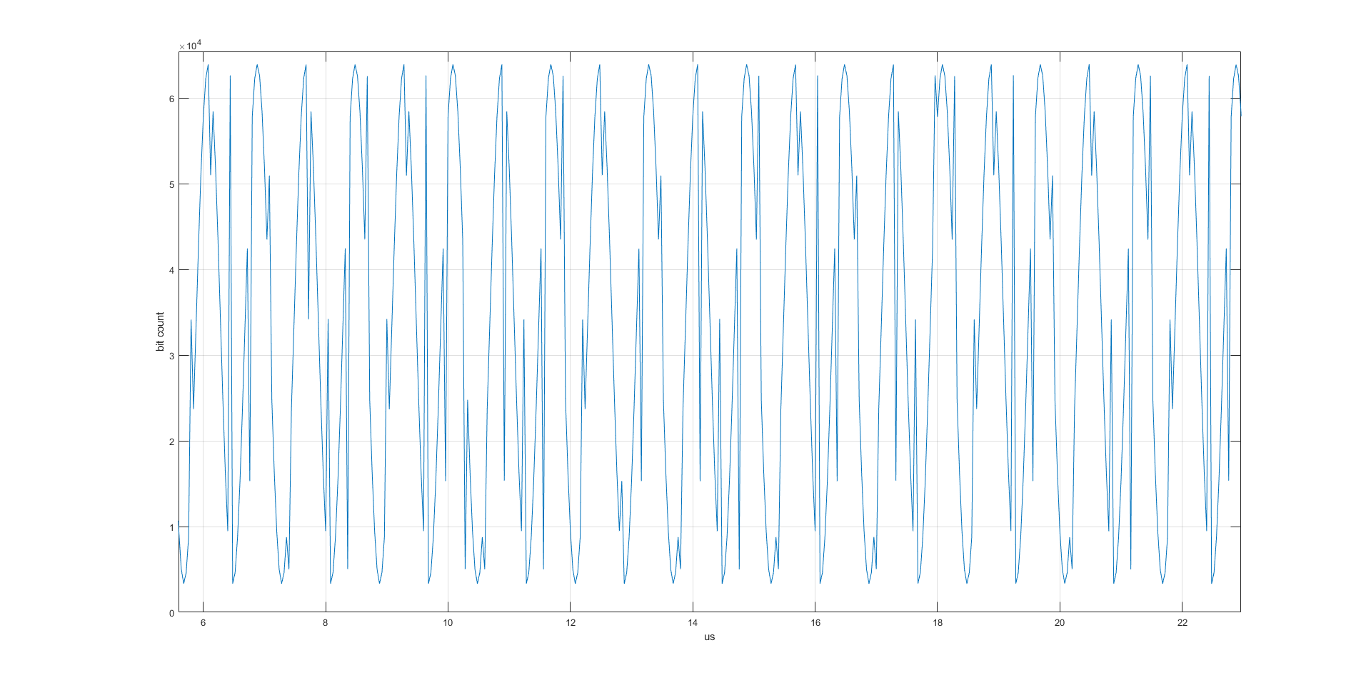
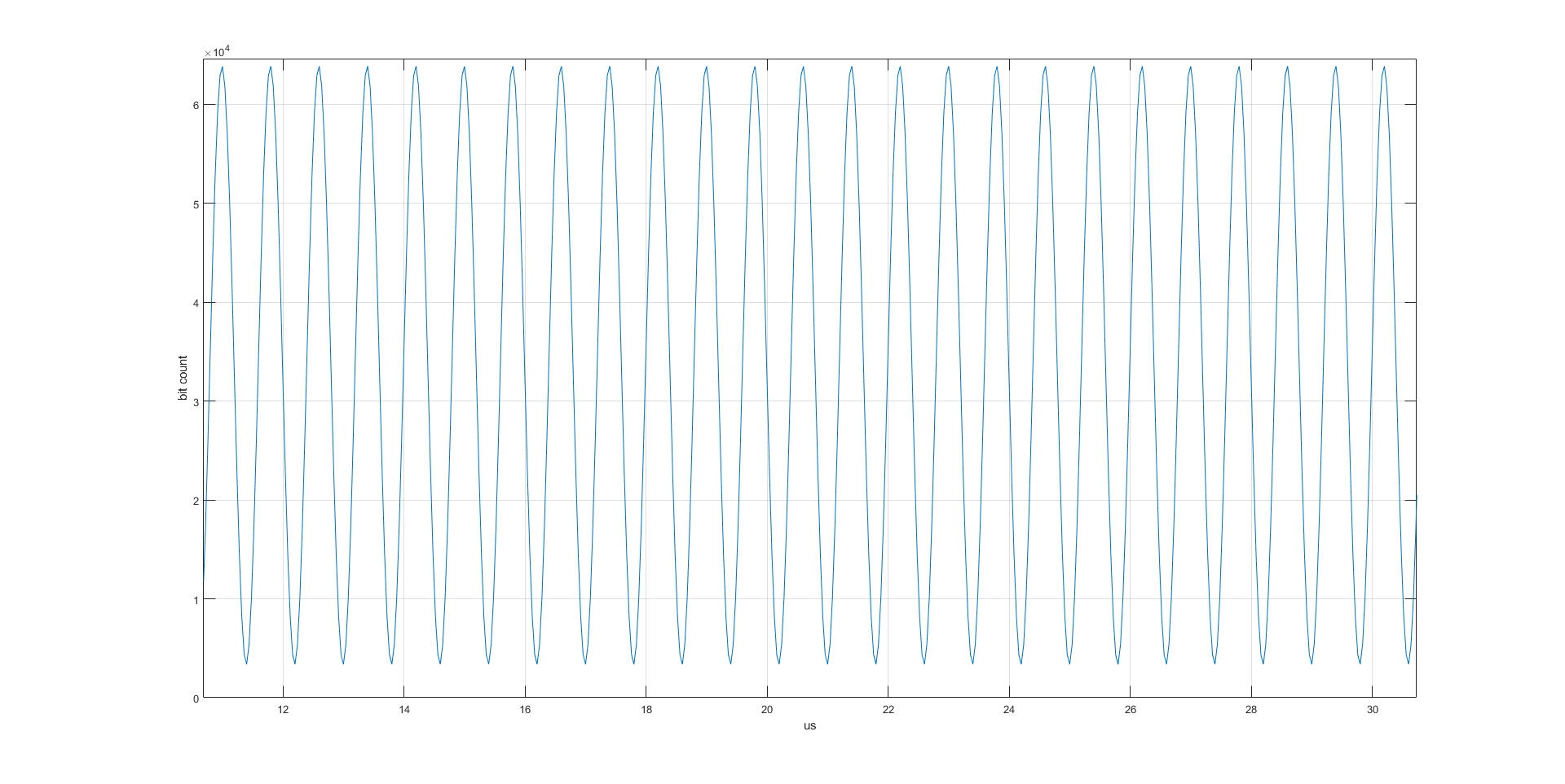
The problem is that after each compilation the timings of the I/Os of the program are substantially changed in an apparent random way, and this affects how the input sinusoid is reconstructed (see the attached pictures).
I tried to apply the "Fast Input Register" assignment in Quartus to the registers of each ADC bit signal, but this is not doing the trick. How can I set timing constraints so that the signal is correctly reconstructed? Do I need to write an .sdc file from scratch? If so, how can I do it? Is there a tutorial/example?
Thanks in advance,
Davide
| 1MHz_notok.png (64.1 KB) 1MHz_notok.png | 1 MHz sinusoid badly reconstructed | ||
| 1MHz_ok.png (53.7 KB) 1MHz_ok.png | 1 MHz sinusoid correctly reconstructed |
Replies (1)
RE: Set timing constraints - Added by Michael Williamson about 7 years ago
Hi Davide,
You really need a constraints file for this to constrain the input timing signals properly based on the ADC datasheet specifications.
There are several (free) online courses available from Intel/Altera about writing timing constraints that I would recommend you take if you are not familiar with the techniques of specifying timing for FPGA design. Here is a link to the first of a starter series on basic timing analysis with Quartus.
https://www.intel.com/content/www/us/en/programmable/support/training/course/odsw1115.html
Where is your CLOCK_20 coming from? If it is from an external clock and being fed into the design you absolutely need a constraints file. At a minimum, you would need a clock spec in your SDC file similar to this:
create_clock -period "20 MHz" [get_ports CLOCK_20]
If you haven't specified the relationship of the input data signals to the clock edge you are using to latch the data, you may not be honoring setup/hold times of the input flip flops. At 20 Mhz, it should be easy to meet the specs. A common error is to sample on the same edge of the clock as the data is output (so you are trying to latch while the data is changing from the source). Often, particularly with slow data rates, simply changing the edge of the clock (inverting it) used to capture the data will resolve capture problems.'
Similarly for the output, if you are clocking the data out on the same clock edge as the DAC is trying to sample, you may cause problems with the DAC.
If you need further assistance, we could support you with a small contract.
-Mike

