HPS/FPGA shared external memory
Added by Maxim Kanevsky about 2 months ago
Dear Sir/Madame,
I would like to create my own design based on mitysom-a5e-ref-base, but with shared between HPS/FPGA external memory. The purpose of this is to exchange data between HPS and FPGA. We would like to try this and see if this can work for our project.
In the example design (mitysom-a5e-ref-base) is used by HPS and it is implemented by "hidden" emif_io96b_hps.qsys where I can "dive", but I can't modify it. I'm just trying to add to the AVMM interface to the FPGA User Logic to be able to access to the External Memory. Please see the attached Block Diagram of what I'm trying to implement.
Can you please suggest the easiest way, with minimum modifications of existing example project, or maybe you can share such example if you already have.
Thanks in advance!!
Max
Replies (5)
RE: HPS/FPGA shared external memory - Added by Mike Fiorenza about 2 months ago
Hi Max,
Yes, this is possible on the Agilex 5 platform, but the external memory connected to the HPS EMIF is not intended to be modified directly through the hidden emif_io96b_hps.qsys block.
For FPGA logic to exchange data with the HPS through shared external memory, the recommended approach is to access HPS-owned memory through one of the HPS/FPGA bridges:
- FPGA-to-HPS bridge, where FPGA logic accesses memory or peripherals through the HPS address space.
- FPGA-to-SDRAM bridge, where FPGA logic can access the HPS SDRAM region more directly, depending on the system configuration.
These bridges are described in the Agilex 5 Technical Reference Manual:
https://docs.altera.com/r/docs/814346/current
The easiest path with minimum modification to the existing reference design would be to start from our DMA example project. That design already demonstrates FPGA-side logic exchanging data with HPS memory using the FPGA-to-HPS bridge. It should provide a good reference for how to connect the FPGA user logic into the HPS memory path without modifying the hidden HPS EMIF subsystem directly.
So rather than trying to add an AVMM port inside emif_io96b_hps.qsys, we recommend using the existing bridge infrastructure and following the DMA example as the starting point.
- Mike
RE: HPS/FPGA shared external memory - Added by Maxim Kanevsky about 2 months ago
Hello Mike,
Thanks a lot for your answer. I've found the same after I posted the question...
Thanks,
Max
RE: HPS/FPGA shared external memory - Added by Maxim Kanevsky about 2 months ago
Hello again,
I've created a project based on mitysom-a5e-ref-base project.
We made following modifications:
- we added FPGA to SDRAM Subordinate Bridge into HPS Subsystem
- we added AVMM to AXI4 Bridge (because all of our modules are AVMM=Avalon Memory-Mapped based)
- we added some AVMM traffic generator that sends Write and Read transactions to F2S Port
- we added Signal Tap to look on this bus (F2S AVMM)
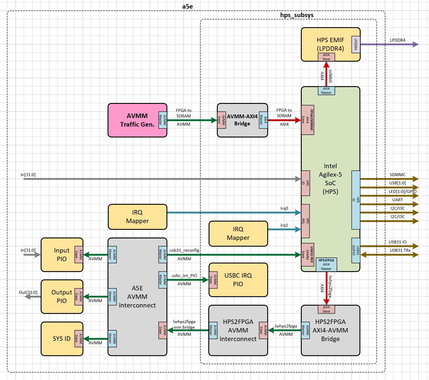
Please see Block Diagram of what we did attached.
base_F2S.JPG
We are running this project on MitySOM and not sure regarding the next steps. How we are accessing to the Memory?
According to Figure 294. Block Diagram (High Level) in 814346 document, there is Multi-Port Front End NoC that needs to be configured. Have you ever used this port or maybe you can point us little bit to what to do??
Thanks,
Max
| base_F2S.JPG (262 KB) base_F2S.JPG |
RE: HPS/FPGA shared external memory - Added by Maxim Kanevsky about 2 months ago
Sorry, forgot to mention, as you suggested, ve tried first DMA example design and we tried to run it. But for now we are interesting in shared memory access, so that's why we are trying FPGA to SDRAM
RE: HPS/FPGA shared external memory - Added by Mike Fiorenza about 2 months ago
Hi Max,
Just to make sure we're aligned on the DMA example — what it demonstrates is really the same use case you're after: exchanging data between the FPGA and the ARM through HPS DDR. The example uses the F2H (FPGA-to-HPS) path. The read/write mSGDMA masters connect to the SoC's fpga2hps port through an ACE5Lite Cache Coherency Translator with a base address of 0x0, so FPGA accesses land in HPS DDR at their natural physical addresses. On the Linux side, the device tree overlay (dma_example.dtso) reserves 256 MB at 0x90000000 as a shared-dma-pool that the userspace app allocates from via /dev/dma_heap.
The DMA example does: FPGA writes data -> HPS DDR -> HPS reads and verifies the data (HPS can read shared data); HPS writes data -> HPS DDR -> FPGA reads and verifies the data (FPGA can read shared data)
Either bridge will get you into shared HPS memory — F2H and F2SDRAM both end up at the EMIF through the Multi-Port Front End NoC. The difference is what they traverse first: F2H goes through the HPS interconnect (and, in our example, an ACE5Lite translator) before reaching the MPFE, while F2SDRAM goes straight to the MPFE.
F2H with the ACE5Lite Cache Coherency Translator: lets FPGA transactions participate in the HPS coherency domain, so software running on the ARM doesn't need to clean/invalidate caches around shared buffers. The tradeoff is the coherency hardware and the HPS interconnect hop add latency and consume some bandwidth budget. However, my understanding from Altera is this only works in one direction (HPS -> FPGA), therefore, cache maintenance is still needed for the (FPGA -> HPS) direction. The kernel shim I have wrote in the DMA example handles the cache maintenance in both directions. It is still on my list to validate if any of these cache maintenance becomes no-ops when running / depending on direction. I also have a few updates to the DMA example that should be published with our next release shortly (traffic generator bug, cache maintenance fixes in my kernel shim / DMA write response support). I will keep you posted once I have an update to that example but nothing that should be a show stopper for you to start exercising this path. You have confirmed that you have ran our DMA example to exercise data between the HPS and FPGA in shared DDR. The data errors you ran into when running this example were caused by a bug in my FPGA xor traffic generator, this will be resolved in the next release.
F2SDRAM: goes straight to the MPFE NoC, skipping the HPS interconnect and the coherency machinery. That's the path Altera positions as the high-bandwidth route to EMIF; software has to handle cache maintenance itself.
- Mike

