Carrier Board Design Gotchas
Below are some common design "gotchas" that customers frequently ask about our encounter and are evaluated after boards have been designed in many cases.
Boot Configuration Resistor Details
- A total of 10 Boot Configuration signals are required on any carrier board to have the MitySOM-5CSx module boot properly. If any of these signals are not explicitly set undetermined boot mode settings may be loaded resulting in boot failure.
- The Critical Link Development Board (80-000578) uses a 10-switch DIP-switch packaged for these resistors. Most customers will find a resistor network to be more desirable for "fielded" designs.
- We do recommend that both high and low resistors options be available but only the desired resistors installed in case changes are necessary in the future.
- Additional details available on this wiki page: https://support.criticallink.com/redmine/projects/mityarm-5cs/wiki/Configuration
CSEL
Due to a still current Errata from Altera we recommend any new, or existing, designs utilize CSEL resistor values of '00' only. In short some Altera Cyclone V processors may be prone to this errata and may not boot reliably if a different CSEL value is used.
Recommended Pull Resistors and Voltages on Carrier Board| Config Option | Module Pin # | Pull-Up Value (Ohm) | '1' Voltage | Pull-Down Value (Ohm) | '0' Voltage |
| CLKSEL0 (CSEL0) | Pin 4 | 10K | 3.3V | 1.1K | GND |
| CLKSEL1 (CSEL1) | Pin 10 | 10K | 3.3V | 1.1K | GND |
BSEL
Critical Link Development Kit boards ship with the BSEL[2:0] values as '101' to boot from the SD card interface.
Supported BSEL options:
001 - FPGA
    010 - 1.8V NAND
    101 - 3V SD/MMC
110 - 1.8V SPI or QSPI (48MB, 32MB and 16MB QSPI NOR)| Config Option | Module Pin # | Pull-Up Value (Ohm) | '1' Voltage | Pull-Down Value (Ohm) | '0' Voltage | Note |
| BOOTSEL0 (BSEL0) | Pin 14 | 10K | 3.3V | 1.1K | GND | |
| BOOTSEL1 (BSEL1) | Pin 249 | 10K | 1.8V | 1.1K | GND | This pin has a series resistor on the module, PCN20150727000 |
| BOOTSEL1 (BSEL2) | Pin 253 | 10K | 1.8V | 1.1K | GND |
MSEL
Critical Link Development Kit boards ship with the MSEL[4:0] values as '00000'.
Recommended Pull Resistors and Voltages on Carrier Board| Config Option | Module Pin # | Pull-Up Value (Ohm) | '1' Voltage | Pull-Down Value (Ohm) | '0' Voltage |
| MSEL0 | Pin 29 | 1.1K | 3.3V | 0 | GND |
| MSEL1 | Pin 45 | 1.1K | 3.3V | 0 | GND |
| MSEL2 | Pin 51 | 1.1K | 3.3V | 0 | GND |
| MSEL3 | Pin 57 | 1.1K | 3.3V | 0 | GND |
| MSEL4 | Pin 36 | 1.1K | 3.3V | 0 | GND |
SD card Pull-up Resistors
After initial MitySOM-5CSx carrier board designs (80-000578 Revision 4 or below) we were made aware of a design requirement/recommendation from Altera in regards to the SD card interface.
As of October 13, 2014 Altera updated their "Cyclone V Family Pin Connection Guidelines" to include ~10k pull-up resistors on both the SDMMC_CMD and SDMMC_D0 signals. This document - PCG-01014.pdf (Page 35 in particular). Any recent critical Link MitySOM-5CSx development kits include this change and you should ensure that it has been added to any custom carrier boards.
Real Time Clock (RTC) Battery Power
- If not using RTC Battery Backup, connect to 2.5V or 3V supply. It is OK to leave this VBAT pin floating for modules of "Dash2" or newer MitySOMs.
- This change is documented in PCN20150626000 found on the module PCN page: https://support.criticallink.com/redmine/projects/mityarm-5cs/wiki/Errata_and_Module_Product_Change_Notifications
- The Cyclone V monitors the battery voltage
- If tied to GND, SOM will not boot
- If too low, the Fabric may not configure (even through JTAG) -- Note that this issue is limited to 5CSX-H6-42A devices with a "Dash1" revision (see above)
Ethernet PHY Routing
Customers should always follow industry best practices when routing/laying-out their Ethernet PHY interface both from the MitySOM-5CSx connector to the PHY and from the PHY to their RJ45 interface. Some recommendations are as follows:
RGMII Layout suggestions:- Keep the wide RGMII bus side of the PHY short - the differential pairs on the connector side of the PHY are less susceptible to crosstalk and noise
- Match the lengths
- Spacing of 3W (3 times the trace width) is sufficient to have effectively no cross-talk
- Most importantly, keep the clock lines clean
- Ensure there is a continuous GND plane under the RGMII routes and GND vias near any layer transitions for the signal routes to provide a good return current path
- Use a target characteristic impedance of 50ohm for the RGMII traces
- Place the smallest bypass caps closest to the PHY power pins
- For best results: on the bypass caps, use vias to the side of the cap footprint instead of the end to minimize ESL parasitics and have the power travel from the power plane, past the cap and to the PHY.
KSZ9031 PHY Address Usage with 1.8 DVDDH
Please see the note in section 9.0 of the KSZ9031 datasheet (http://ww1.microchip.com/downloads/en/devicedoc/00002117f.pdf) to ensure proper latching of the Phy ID. Typically not a concern with a single Phy however if multiple MDIO devices are on the bus this could cause an error.
USB PSW/USB1_PS_ON Pull-down/up Resistors
Critical has determined that the original MitySOM-5CSx Development Kit baseboard design utilized a 2.2k ohm pull-down resistor for the USB1_PS_ON (Pin 246) signal which was found to be problematic for some modules at higher temperatures. As such we highly recommend customers utilize a 10K pull down for existing designs based upon our 80-000578 baseboard design (Rev9B or lower) or for new designs a value from 60k to 100k ohms if possible. The resistor in question is R411 from our dev board design.
Please seen the PCN/Errata sections of the wiki for more details.
DDR3 Clock Source (X101 On 80-000578 Schematics)
- The DDR3 clock source is only needed when customers want to utilize the on-module FPGA DDR3 direct memory (256MB or 512MB in size).
- If using a single-ended CLK2DDR, connect to _P pin because this has a direct connection to the PLL.
- This clock input is specifically named CLK2DDR because it is the only clk input that will meet the DDR clock constraints for the FPGA DDR interface on the MitySOM. Module Pins #117 and 119.
- On designs that have a module that do not include that memory or it will not be utilized this clock source can be omitted.
- CLK2DDR input is NOT for the main DDR3 system memory (512MB, 1GB or 2GB) that is accessible by both the HPS and FPGA.
Fabric Bank Voltages
- Bank 3B (Pin 134), 4A (Pin 48) and 8A (Pin 176) bank voltages must be provided by the baseboard
- If >2.5V on Bank3B or Bank4A, Both Bank 3B and 4A need to be the same
- For <=2.5V bank voltages, the Bank3B and 4A voltages can be different
- Bank3A/5A/5B (Pin 181)
- Is a floating pin for MitySOMs with FPGA DDR
- Expanded I/O SOMs need the Bank3A/5A/5B voltage provided by the baseboard
- All Bank7x banks have fixed voltages
- USB PHY and QSPI interfaces are internal and on 1.8V rails
- Bank7B is 1.8V I/O. For convenience, the MitySOM provides a 1.8V rail (1.8V_VIO - Pin 273) for the Bank7B I/O drivers.
- Bank7C is 3.3V I/O.
- The Predriver voltage is selected internally based on the I/O bank voltage provided in the design
3.3V I/O Interfaces
- Altera recommends enabling the internal protection diodes if running a bank on 3.3V I/O levels
According to the Cyclone V Device Handbook (https://www.altera.com/content/dam/altera-www/global/en_US/pdfs/literature/hb/cyclone-v/cv_5v2.pdf) it is recommended that the clamp diodes be enabled for 3.3V IO standards as shown on Page 5-19 and 5-20 under the "Guideline: Observe Device Absolute Maximum Rating for 3.3V Interfacing". The clamp diodes are recommended to "limit the overshoot and undershoot voltage at the I/O pins". Table 5-24 of the Handbook shows the settings/defaults for the "On-Chip Clamp Diode". Note that the need for the clamping diodes is very design dependent and not all designs may require them.
If it is determined that the clamping diode option needs to be enabled for a pin (or set of pins) they can be added through Quartus using the Assignment Editor.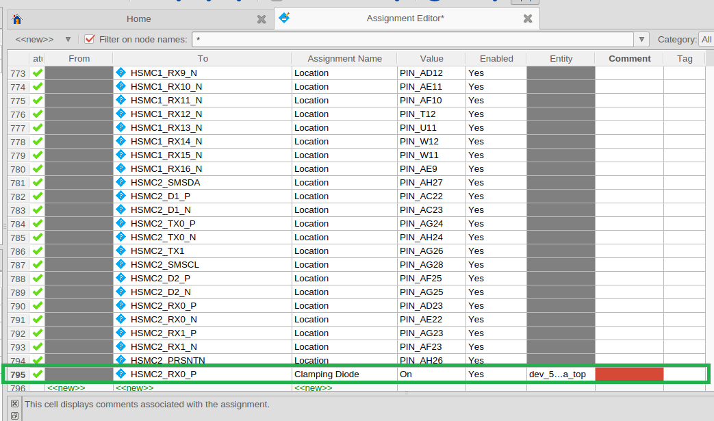
- Add a new assignment for the Pin in question ("TO" column)
- Select "Clamping Diode" from the "Asignment Name" drop-down menu
- Select a Value of either "on" or "off"
- It should be "enabled"
Additionally page 459 of the "Quartus Settings File Reference Manual" covers a little detail about the "CLAMPING_DIODE" option (https://www.altera.com/content/dam/altera-www/global/en_US/pdfs/literature/manual/mnl_qsf_reference.pdf).
USB Debug UART RX
If a design incorporates the UART to USB (FT230XS) for the Debug serial interface we have found that when this interface is not connected to a PC the UART0_RX signal can "float" causing the boot process of the module to be halted in some instances.
We recommend adding a "weak pull up" to the UART0_RX signal in your pre-loader software if you implement a USB to UART device. Alternatively you can add a weak pull-up to the UART0_RX signal of your carrier board instead of the software change.
KSZ RGMII Phy Implementation Options
Please see this Wiki Page, KSZ RGMII Phy Design Considerations, for details concerning the KSZ 9021/9031/9131 family of Ethernet Phy's such as the below:- KSZ Phy 1.2V Supply Requirements
- Current Requirements
- Supply Options
- MOSFET (Phy controlled through LDO_O pin)
- External LDO
- External DC-DC converter
- Pin-Out differences between KSZ 9021, 9031 and 9131 Phys
- Mode differences between KSZ 9021, 9031 and 9131 Phys