FPG DDR3 Memory Pin Assignment
Added by Anonymous over 12 years ago
Hi,
Can you please provide the pin assignment for the optional FPGA DDR3 memory please?
Thanks!
Jack
Replies (8)
RE: FPG DDR3 Memory Pin Assignment - Added by Daniel Vincelette over 12 years ago
Hi Jack,
I have attached a TCL file that will setup the pin assignments for the FPGA DDR.
Dan
| mityarm_5csx_dev_board_fpga_ddr_setup.tcl (2.32 KB) mityarm_5csx_dev_board_fpga_ddr_setup.tcl | MityARM 5CSX FPGA DDR assignments |
RE: FPG DDR3 Memory Pin Assignment - Added by Anonymous over 12 years ago
Hi Dan,
Could you provide the TCL file for the IO Standard as well please?
Thanks!
Jack
RE: FPG DDR3 Memory Pin Assignment - Added by Daniel Vincelette over 12 years ago
Hi Jack,
The IO Standard TCL file should be auto-generated by the tools.
To run it from Quartus:
1) Go to Tools->TCL Scripts
2) In the TCL Scripts window you should see multiple tcl scripts, there should be one that looks like mityarm_5csx_dev_board_fpga_ddr_p0_pin_assignments.tcl, select that one. I named the FPGA DDR controller fpga_ddr in my qsys project so that might be different in your project.
3) Click Run
This will go set your IO Standards.
Dan
RE: FPG DDR3 Memory Pin Assignment - Added by Anonymous over 12 years ago
Hi Dan,
I ran the tcl script that you attached on this thread.
But when I tried to compile, it gives me errors like the following:
Error (169026): Pin FPGA_DDR_A0 is incompatible with I/O bank 5A. It uses I/O standard 2.5 V, which has VCCIO requirement of 2.5V. That requirement is incompatible with bank's VCCIO setting or other output or bidirectional pins in the bank using VCCIO 1.35V.
Jack
RE: FPG DDR3 Memory Pin Assignment - Added by Daniel Vincelette over 12 years ago
Hi Jack,
Did you also run the IO Standard TCL file generated by the tools?
Dan
RE: FPG DDR3 Memory Pin Assignment - Added by Anonymous over 12 years ago
Hi Dan,
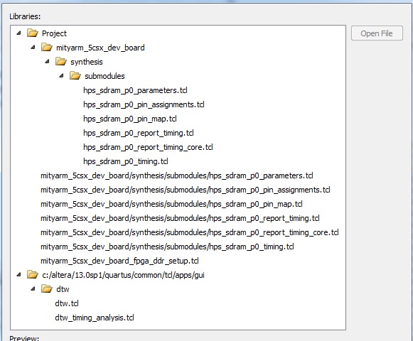
I don't see the TCL file that you are referring to. All the tcl files that I have are for HPS DDR not FPGA except for the one that you attached.
I attached the a print screen showing all the files.
Jack
RE: FPG DDR3 Memory Pin Assignment - Added by Daniel Vincelette over 12 years ago
Hi Jack,
Hmm, are you using the DDR SDRAM Controller with UniPHY in your QSYS project?
Also with this first release of the 5CSX SOM there is a special hardware modification that is needed in order to get the FPGA DDR to work, which is explained in the Errata. If this SOM wasn't bought with special orders to add this modification the FPGA DDR will not work. If this mod is installed there will be a long wire on the back of the SOM attaching to one of the pins on the edge connector.
In one of our current designs we are using just the HPS DDR, which is running at a fairly high bandwidth and working quite well. We have found that using the HPS DDR is simpler and easier to setup. Is there a design constant that requires the use of the FPGA DDR or might it be possible that you could get away with using just the HPS DDR?
Dan
RE: FPG DDR3 Memory Pin Assignment - Added by Anonymous over 12 years ago
Hi Dan,
We would like to use the HPS DDR as well, but as you can see from my numerous posts, we are really stuck on memory write to multiple addresses. So while you guys are preparing an example for writing to the HPS DDR, we will have to explore other options.
We were using the Xula2 FPGA board in one of our prototypes, and that board was easy to use as they provided documents and examples on their memory controller. So we have all our algorithm ready, we just need to know from you guys how to work the memory controller. We have been stuck on this for nearly a month now, so we would appreciate your help ASAP.
Thanks!
Jack

