MityDSP-L138F Mounting Holes (Posted on behalf of a customer)
Added by Angela Newman about 14 years ago
I’m designing a carrier board to host the MityDSP-L138F and would like to use the plated through holes at the edge of the module to solidly mount it to my carrier board. I know the location of the plated through holes relative to the module edges (shown in Fig 1 of the carrier board design guide), but I cannot determine where to place the plated through holes on the carrier board because I have no point of reference, or origin, as a reference point. I’m assuming you guys figured this out already since you have the plated through mounting holes correctly placed on your industrial I/O board.
Can you tell me the center coordinates of the two mounting holes relative to the center of pin 1 of the SODIMM connector on the industrial I/O board? Using that information I should be able to place the holes correctly on my carrier board.
Replies (10)
RE: MityDSP-L138F Mounting Holes (Posted on behalf of a customer) - Added by Thomas Catalino about 14 years ago
I've attached the requested drawing, does this address your needs?
Tom
| Omap_MH.pdf (16.9 KB) Omap_MH.pdf |
RE: MityDSP-L138F Mounting Holes (Posted on behalf of a customer) - Added by Wade Calcutt almost 14 years ago
Thanks Tom, this is exactly what I needed.
RE: MityDSP-L138F Mounting Holes (Posted on behalf of a customer) - Added by Emmett Bradford almost 14 years ago
Hi Tom,
I hate to be a pain, but could you dimension this from the centerline of the connector, or give me a dimension from the pad 1 center to the centerline?
Different manufacturers suggest slightly different pad footprints, but the centerline is the centerline.
I am comparing this to Figure 2 of the MityARM-1808F datasheet and something's off.
Thanks,
Emmett
RE: MityDSP-L138F Mounting Holes (Posted on behalf of a customer) - Added by Alexander Block almost 14 years ago
Emmett,
Sorry about the late reply on this issue. Hopefully you have resolved it satisfactorily but if not I believe I have the dimension you requested:
From the Center Line of Pin 1 to the Center Line of the SODIMM connector is 161mil.
Thank you for pointing out that there was a discrepancy between the footprint and the datasheet. The issue found was that in reality the footprint should have had the outside edge of the MityDSP-L138 module moved in towards the connector 20mil due to insertion into the connector. Originally we had that outline of the module start at the center-line of the connector but in reality that was incorrect. So the outline was moved and the holes stayed in the same place. Everything now makes sense to me and hopefully the attached PDF corrects the issues you found.
If this is still wrong please let me know.
Thanks,
Alex
RE: MityDSP-L138F Mounting Holes (Posted on behalf of a customer) - Added by Alexander Block almost 14 years ago
Now I've attached the updated PDF.
Alex
| L138_MH.pdf (104 KB) L138_MH.pdf | L138 Mounting Hole Mechanical Dimensions |
RE: MityDSP-L138F Mounting Holes (Posted on behalf of a customer) - Added by Emmett Bradford almost 14 years ago
Thanks Alex
That shows everything I need.
RE: MityDSP-L138F Mounting Holes (Posted on behalf of a customer) - Added by Wade Calcutt almost 14 years ago
The drawing you provided highlights a keep-out area for high profile components. What is the maximum component height allowed in this area? Is it 1.60 mm as specified in Figure 2 of the carrier board design guide?
Thanks.
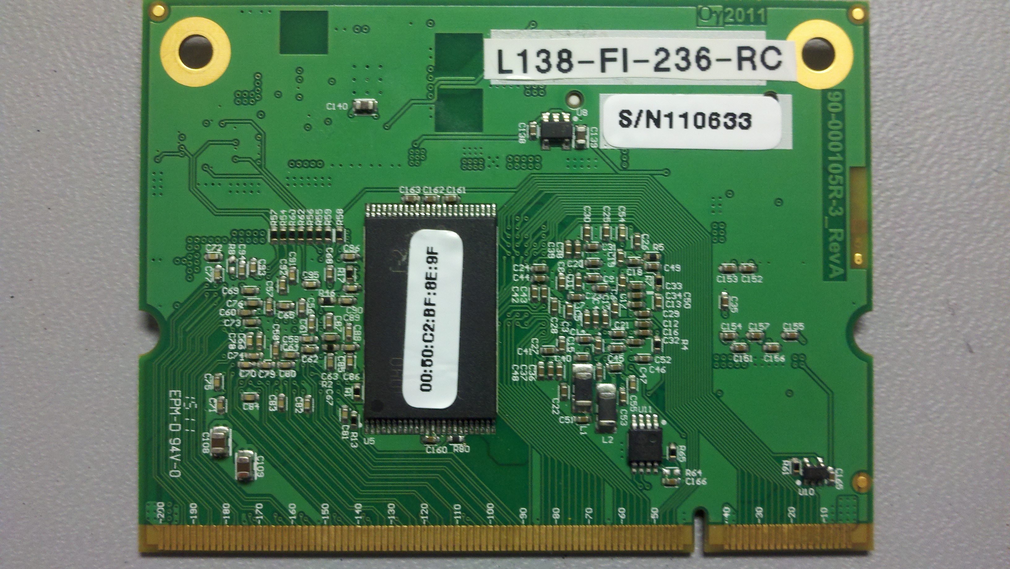
RE: MityDSP-L138F Mounting Holes (Posted on behalf of a customer) - Added by Michael Williamson almost 14 years ago
Short answer is yes, 1.6mm maximum height. And you should probably hold to that height for the entire area below SOM as per the design guide, as there are a couple of small IC's outside the area in the drawing that was posted and there is an SMT NAND part (highest part on the backside of the module) which seems to extend beyond the region in the figure. I need to circle back with Alex and our CAD guys about that keep out area in the drawing, Wade, I'm not sure that's correct.
I've attached a photo of the backside of the L138F for your reference. All of the small IC's are pretty much the same height as the NAND part.
-Mike
| 2012-08-23_08-24-29_757.jpg (2.05 MB) 2012-08-23_08-24-29_757.jpg | Back of MityDSP-L138F |
RE: MityDSP-L138F Mounting Holes (Posted on behalf of a customer) - Added by Michael Williamson almost 14 years ago
We may have a STEP model of the module, let me see if I can get that published.
RE: MityDSP-L138F Mounting Holes (Posted on behalf of a customer) - Added by Wade Calcutt almost 14 years ago
Mike, thanks for the quick response.
A STEP model is currently available at [http://support.criticallink.com/redmine/attachments/1293/MityDSP-L138F.step] unless you're referring to a newer version.
The keep-out area shown in the drawing is about half to a third of the surface area of the module (depending upon the model). I designed a carrier board to accommodate the 1.6 mm height constraint requirement for the entire area under the module but I wanted to verify that it wasn't an additional height constraint (< 1.6 mm) for that specific area of the module. Based on your answer it sounds like it isn't.
Thanks again for your help.
-Wade

