Forums » Software Development »
FPGA (FIFO) -> DSP (DMA) transfer problem
Added by Kyungguk Bok about 2 years ago
hello.
I am posting because I have a question related to DMA.
The last CCS issue was not resolved, so I am loading the DSP application through ARM. (Thank you to those who helped.)
The work I am currently doing is accumulating data (16 bits, 0 to 8192) through FIFO in FPGA, and when the number reaches 4096, an interrupt is generated through GPIO (directly to DSP without FPGA) with fifo_almost_full, and data is retrieved from FIFO through DMA. I'm working on it.
Before that, we confirmed that data was normally retrieved from FIFO through EMIF, and are in the process of retrieving data by changing to DMA.
Below is the FPGA FIFO source.
fifo_rd_en <= '1';
process(ema_clk)
 begin
 if rising_edge(ema_clk) then
  if i_ema_cs5_n ='0' and i_ema_oe_n ='0' then
  fifo_rd_clk <= '1';
  emd_d_out <= '0';
  else
  fifo_rd_clk <= '0';
  emd_d_out <= '1';
  end if;

  if emd_d_out = '0' then
  io_ema_d <= fifo_dout;
  else -- emd_d_out = '1' then
  io_ema_d <= (others => 'Z');
  end if;
  end if;
end process;

fifo_wr_en <= '1';
process(raw_clk)
 begin
 if rising_edge(raw_clk) then
  if clk_count < 25 then
  clk_count <= clk_count + 1;
  fifo_wr_clk <= '0';
  else
  clk_count <= 0;
  fifo_wr_clk <= '1';
  if data_counter < x"2000" then
  data_counter <= data_counter + 1;
  else
  data_counter <= (others => '0');
  end if;
  end if;
  if fifo_wr_clk = '1' then
  fifo_din <= data_counter;
  end if;
  o_dvi_data <= fifo_din;
 end if;
end process;
o_diode(0) <= fifo_almost_full;
raw_clk is 50MHz. In the above code, we confirmed that data is transmitted normally through EMIF communication (experiment was conducted on DSP by setting address).
Currently, it is only used for DMA, so the address is not set first, and output is performed only with EMIF CS5 and RD Enable signals.
Below is the DSP code.
//for DMA
unsigned short BUFFER_SIZE = 4096;
unsigned short* src = (unsigned short*)(0x66000010);
unsigned short* dst = (unsigned short*)(0x11800000);

unsigned short srcBuffer[4096];
unsigned short destBuffer[4096];
//for interrupt
unsigned int *GPIO_BINTEN01 = (unsigned int *)0x01E26008;
unsigned int *GPIO_DIR01 = (unsigned int *)0x01E26010;
unsigned int *GPIO_SET_RIS_TRIG01 = (unsigned int *)0x01E26024;
unsigned int *GPIO_CLR_RIS_TRIG01 = (unsigned int *)0x01E26028;
unsigned int *GPIO_CLR_FAL_TRIG01 = (unsigned int *)0x01E2602C;
unsigned int *GPIO_INTSTAT01 = (unsigned int *)0x01E26034;

void main()
{
 //for interrupt
 tcDspSyscfg::SetPinMuxConfig(pins);

 HWI_eventMap(6, 65);

 HWI_dispatchPlug(6, (Fxn)isr_printf, -1, NULL);

 *GPIO_BINTEN01 = 0x00000001;
 *GPIO_DIR01 = 0xFFFFFFDF;
 *GPIO_SET_RIS_TRIG01 = 0x00000001;
 *GPIO_CLR_FAL_TRIG01 = 0x00000001;
 C62_enableIER(1 << 6);

 //for DMA
 dma=tcDspQDMA::GetInstance();
 dma->Initialize(7);
 while(1)
 {
 }
}

void isr_printf(tcGpio *apThis, unsigned int Bank, unsigned int Offset, void *apUser)
{

 memset(destBuffer, 0, sizeof(destBuffer));

 dma -> BlockTransfer(&myHandle, src, dst, 4096, EDMA_OPT_ESIZE_16BIT, EDMA_OPT_PRI_HIGH,0);
 SEM_pend(myHandle, SYS_FOREVER);

 memcpy(destBuffer, dst, 4096 * sizeof(unsigned short));
}
When fifo_almost_full operates as an interrupt, dma is activated to receive data.
The data received from fifo is transmitted to ARM through IPC, and ARM checks the data through its own GUI using UDP communication.
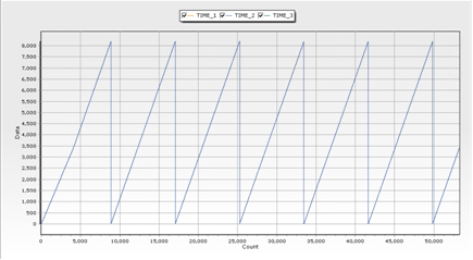
Below, when FIFO data was received via EMIF, the data was checked using the GUI and the graph was displayed normally.
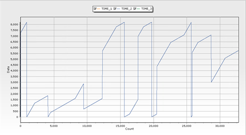
When FIFO data is transmitted through DMA, the data is not transmitted in order as shown below, or the same value is transmitted 2 to 3 times.
I spent a lot of time trying to solve the above problem, but I don't know the cause.
I am attaching the code, so please let me know the solution.
| picture479-1.png (54.5 KB) picture479-1.png | EMIF | ||
| picture479-2.png (51 KB) picture479-2.png | DMA |
Replies (5)
RE: FPGA (FIFO) -> DSP (DMA) transfer problem - Added by Jonathan Cormier about 2 years ago
The fpga guys can step in if I've missed something but it looks to me like your missing cache invalidate calls. If the DMA engine is modifying RAM outside of the DSPs knowledge, then the DSP needs to be informed that its cache of that memory is invalid and needs to be read again.
Please refer to Cache_and_Memory and let us know if you have any additional questions. And if this helps.
RE: FPGA (FIFO) -> DSP (DMA) transfer problem - Added by Kyungguk Bok about 2 years ago
Thank you for answer.
As you suggested, read Cache_and_Memory and
We proceeded by modifying the source as shown below.
void isr_printf(tcGpio *apThis, unsigned int Bank, unsigned int Offset, void *apUser)
{

 dma -> BlockTransfer(&myHandle, src, dst, BUFFER_SIZE , EDMA_OPT_ESIZE_16BIT, EDMA_OPT_PRI_HIGH,0);//ReadFromFIFO
 SEM_pend(myHandle, SYS_FOREVER);

 memset(srcBuffer, 0, sizeof(srcBuffer));
 memset(destBuffer, 0, sizeof(destBuffer));

 BCACHE_inv(dst, BUFFER_SIZE * sizeof(unsigned int), TRUE);
 BCACHE_inv(src, BUFFER_SIZE * sizeof(unsigned int), TRUE);
 BCACHE_wait();

 memcpy(destBuffer, dst, BUFFER_SIZE * sizeof(unsigned int));
}
(Change data type from short to int)
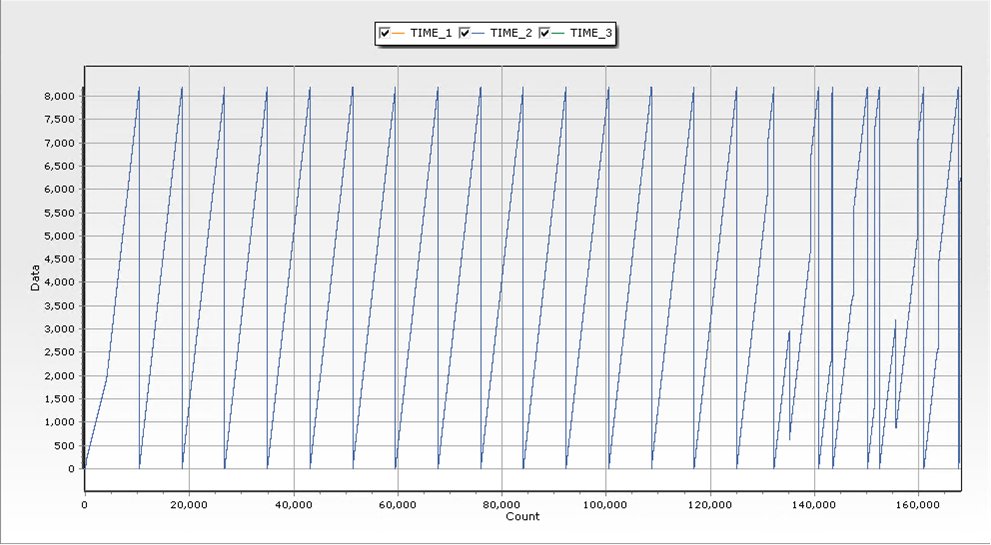
Afterwards, as a result of measuring using the GUI, data seemed to be transmitted normally at first, but as time went by, it was confirmed that strange data was being transmitted. What kind of problem is this?
| picture789-1.png (298 KB) picture789-1.png | DMA |
RE: FPGA (FIFO) -> DSP (DMA) transfer problem - Added by Gregory Gluszek about 2 years ago
Hello,
Based on the FPGA code you shared I believe that the primary issue you are having is that your FPGA code requires transitions on i_ema_cs5_n or i_ema_oe_n in order to read out new FIFO samples. These transitions are most likely happening for every read when not using a DMA, however, once DMA is being used you may have burst of read requests where i_ema_cs5_n and i_ema_oe_n are both '0' for multiples ema_clk cycles and your FPGA code does not generate an edge on fifo_rd_clk and the FIFO will not produce a new sample. (If you have a Xilinx Platform Cable USB II JTAG debugger you should be able to verify if this behavior is happening in the FPGA or not using Chipscope debugging tool Xilinx offers.)
I believe that a quick fix would be to feed the FIFO a proper clock on the read side (e.g. ema_clk) and drive fifo_rd_en high based on i_ema_cs5_n ='0' and i_ema_oe_n ='0'.
However, a more complete fix would be to consider following the structure we use for our FPGA designs. I would recommend using fpga/vhdl/MityDSP_L138_top.vhd in our MDK (which can be downloaded at https://support.criticallink.com/redmine/projects/arm9-platforms/files) as a starting point for your FPGA design. Following this structure will allow you to instantiate the idea of multiple "cores" in your FPGA so that you can share the FPGA memory space across a variety of units that offer different functionality (your current example assumes any interaction on the FPGA memory space of the EMIF bus is a FIFO read request). You can look at the fpga/vhdl/base_module.vhd code in the MDK for an example of creating a core and handling reads to a specific register offset. Then when that particular register is read you can trigger a read to your internal FIFO and put return the next sample on the EMIF bus.
Furthermore, regarding the DSP code, I recommend using dma->ReadFromFIFO() instead of dma->BlockTransfer(). ReadFromFIFO() assumes the DMA is reading from src address again and again without incrementing, while dma->BlockTransfer() will increment the source address (and is only working in your current design as you are handling any access on the EMIF bus as a FIFO read. Note that if you were to do a large enough FIFO read in your current design the DMA would start reading outside the FPGA memory space). Also, in the case of dma->ReadFromFIFO(), you only need BCACHE_inv() for your dst, as src is pointing to the FPGA memory space which is not cached. Lastly, since the last argument in BCACHE_inv() is TRUE, you do not need to call BCACHE_wait() as setting that final parameter to TRUE means BCACHE_inv() is already calling said function.
Thanks,
Greg
RE: FPGA (FIFO) -> DSP (DMA) transfer problem - Added by Kyungguk Bok about 2 years ago
Thank you for answer.
We will conduct the above experiment later.
Currently, we are trying to increase the RD Clk speed of FIFO.
MDK_2014-01-13/sw/ARM/u-boot-mitydspl138/board/davinci/mityomapl138/mityomapl138.c
In the file above, the Setup, Strobe, and Hold parts of CS5 were modified.
emif_regs->AB4CR = /* CE 5 address space config register /
(0 << 31) | / Select Strobe /
(0 << 30) | / Extended Wait /
(0x0 << 26) | / Write Setup-1 in EMA_CLK /
(0x0 << 20) | / Write strobe-1 in EMA_CLK /
(0x0 << 17) | / Write Hold-1 in EMA_CLK /
(0x0 << 13) | / Read Setup-1 in EMA_CLK /
(0x5 << 7) | / Read Strobe-1 in EMA_CLK /
(0x0 << 4) | / Read Hold-1 in EMA_CLK /
(0 << 2) | / Turn-Around in EMA_CLK /
(One); / Bus Width (16 bits data bus) */
Setup and Hold have a minimum of 1clk, and Strobe is currently set to 6clk.
The experiment was conducted by modifying the strobe (gradually changed to 6~3clk).
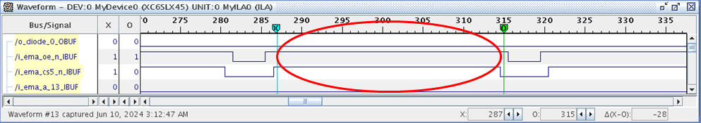
As a result of checking with Chipscope, it was confirmed that CS5 was applied appropriately for the Strobe modification.However, in the photo below, Setup and Hold are set to 1clk, but it is confirmed that 28clk is required between CS5.
I'd like to know what happens in this part.
Is there something I don't know??
| picture416-1.png (89.3 KB) picture416-1.png |
RE: FPGA (FIFO) -> DSP (DMA) transfer problem - Added by Michael Williamson about 2 years ago
There is a cross-bar that sits between EMIFA on the L138 and the DSP / ARM / peripheral masters.
When a read request is generated by the DSP to the EMIFA space, a command/request is generated to the cross-bar controller. The controller has multiple request sources (ARM controller, NAND controller, DMA controller, etc.), and prioritizes the request and eventually executes it. The controller is notoriously slow in processing multiple commands back to back from the DSP. 28 clocks seems long, but may not be unreasonable depending on the back to back transactions.
Is the transaction you are monitoring a DSP memory request or a DMA request? The DSP may require the first transaction to complete before issuing the next transaction, which will result in a stall.
What is your goal? if you are trying to stream high amounts of data from the FPGA to the DSP, I would suggest you consider using the UPP interface instead of the EMIFA interface.

