Customizing the On Board Silicon Labs PLLs
Creating a custom PLL binary configuration file
Download the Silicon Labs Clock Builder Software
The Silicon Labs clock builder software must be used to configure the PLL settings for the SI5338 clock chips. The software can be downloaded from Skyworks website.. We recommend using version 4.17 of ClockBuilder Pro as that's what these instructions were written for. Using a different version of ClockBuilder may result in the PLL not configuring correctly.
Determine Which PLL (U14 or U15) you need to customize
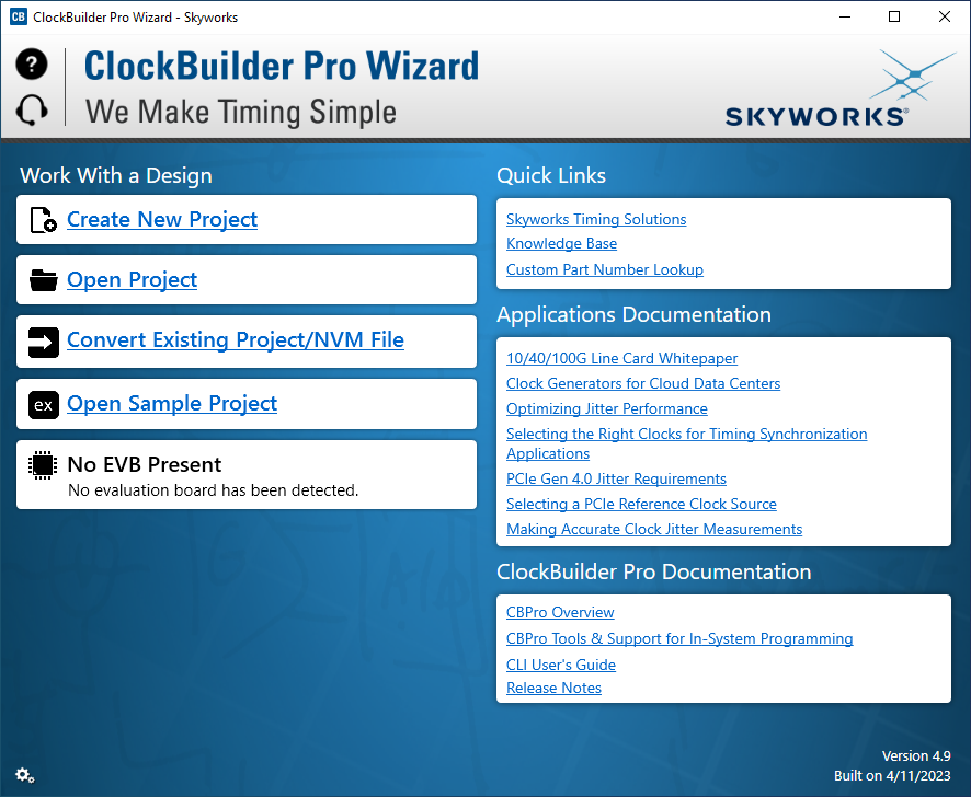
Launch the Clock Builder Application
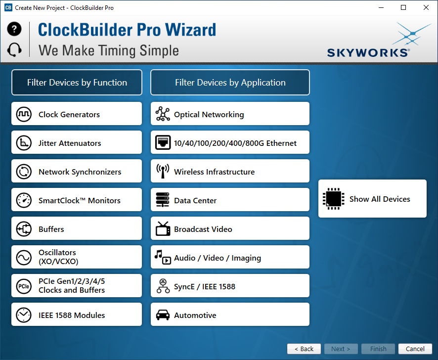
Select "Create New Project" and select the Clock Generators Application
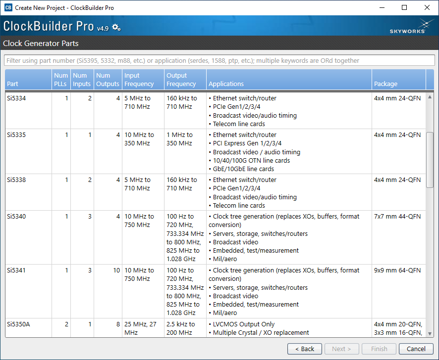
Select the Si5338 Chip
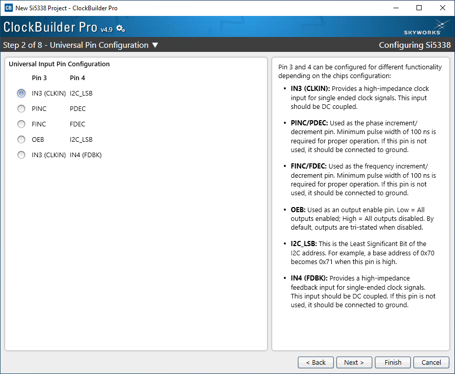
Configure the Pin 3 / Pin 4 to use the IN3 (CLKIN) and I2C_LSB option
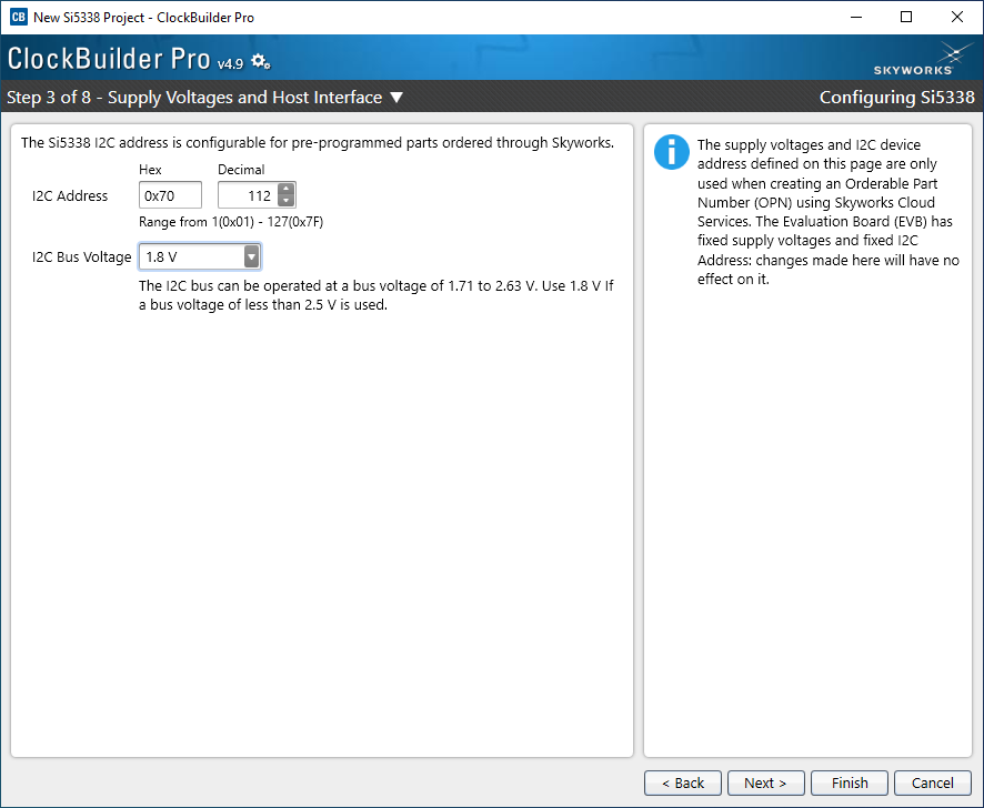
Set the Device Address and I2C Voltage Level
For U14, the I2C address must be set to 0x71. For U15 the I2C address must be set to 0x70.
The I2C Voltage level must be set to 1.8V.
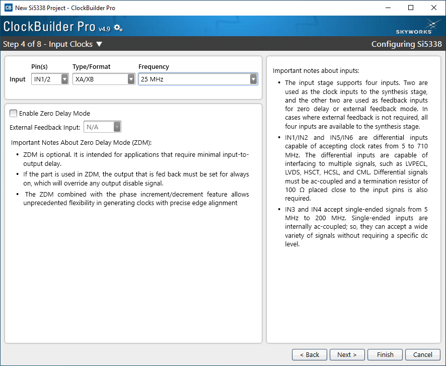
Set the Input Frequency to the PLL to 25 MHz.
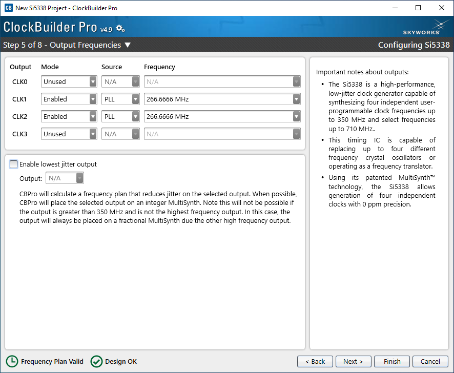
Configure the Clock Frequencies
Check the A10 revision that you are working with. The tables below outline the configuration depending on the revision:
Revision 6 or less| U14 | Frequency | Clock |
| CLK1 | 266.6666 MHz | HPS DDR4 Clock |
| U15 | Frequency | Clock |
| CLK2 | 266.6666 MHz | FPGA EMIF DDR4 Clock |
| U14 | Frequency | Clock |
| CLK1 | 266.6666 MHz | HPS DDR4 Clock |
| CLK2 | 266.6666 MHz | FPGA EMIF DDR4 Clock |
At this point, you should add the additional clock frequencies that you require.
View the SOM clocking section of the datasheet to see the available PLL connections: MitySOM-A10S Datasheet
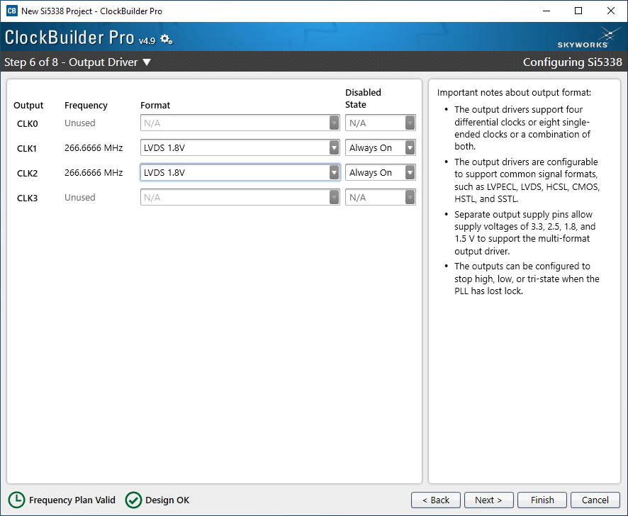
Configure the Output Drivers
For all enabled output clocks, select LVDS with a 1.8V reference voltage.
Skip the phase offset inputs (no phase is required)
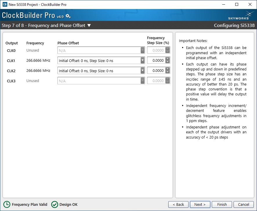
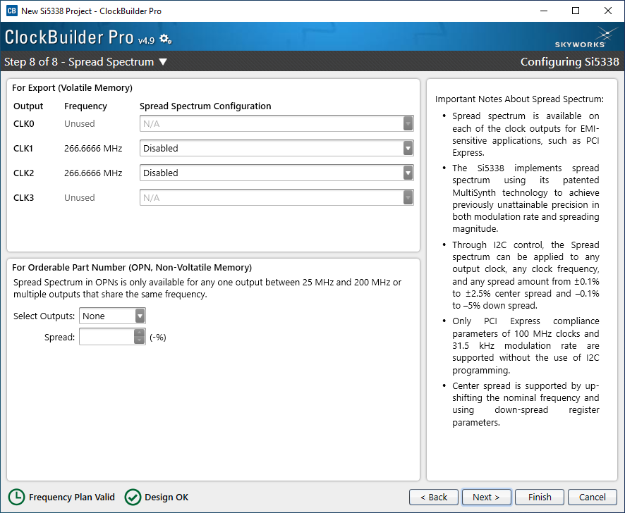
Skip the spread spectrum options
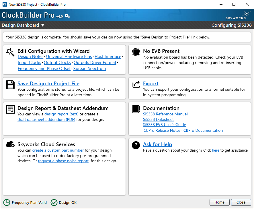
Select Export to save the configuration
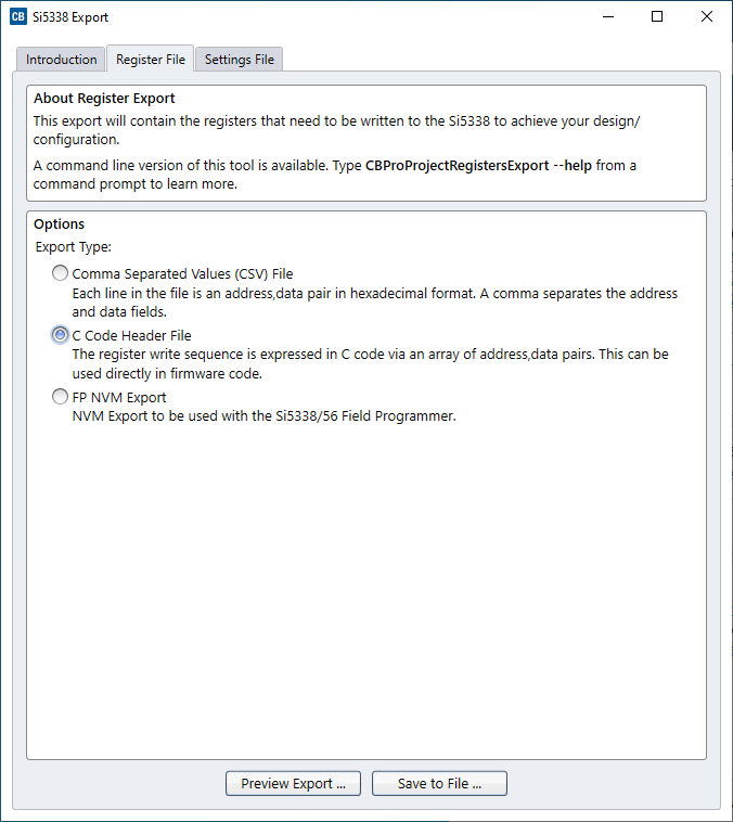
Select the Register File tab and check C Code Header File then press Save to File
Convert the header file into the final expected output binary file
- Rename the c code header file to register_map.h
- Update register_map.h to remove the word code from the following line: Reg_Data const code Reg_Store[NUM_REGS_MAX] = {
-Reg_Data const code Reg_Store[NUM_REGS_MAX] = { +Reg_Data const Reg_Store[NUM_REGS_MAX] = { - Remove the following list from register_map.h:
-{231,0x00,0x00}, - Download the attached gen_regmap.c file for converting the header into the expected binary file
- Move the register_map.h and gen_regmap.c files into the same directory for compilation
- Compile the gen_regmap utility with the following command
gcc gen_regmap.c -o gen_regmap
- Run the compiled utility to generate the binary file with the following command
./gen_regmap
- The utility will output the PLL binary as PLL.bin. Rename this file to U14PLL.bin or U15PLL.bin depending on which PLL it is intended to program.
- Copy the newly created binary onto the FAT partition of the SD card.