MitySOM-A10S Architecture
Top Level Block Diagram
The top level block diagram of the MitySOM-A10S module is illustrated in the figure below. It is possible to update the FPGA, add/remove eMMC, and add/remove 12V main power support.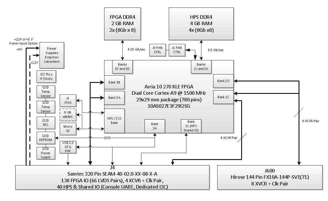
Clocking Diagram
The MitySOM-A10S has multiple oscillators and external PLLs to drive both the HPS and FPGA. There is a dedicated 50Mhz oscillator to drive the HPS reference clock. There are also 2 external 4 port I2C programable PLLs that are used to drive the HPS/FPGA DDR and the transceivers. The SOM clock network is shown in the figure below.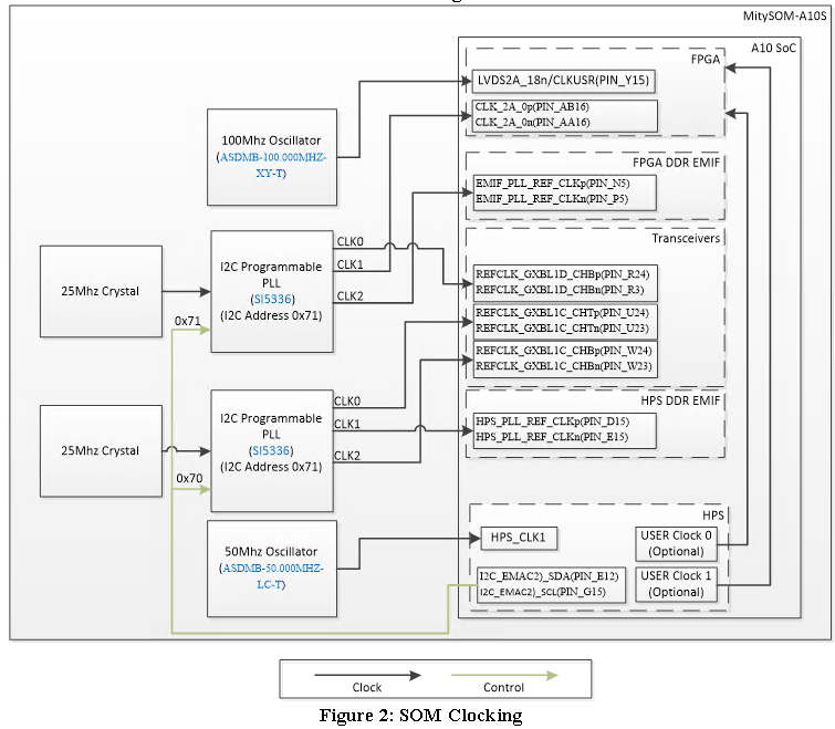
Boot Media Block Diagram
The MitySOM-A10S can boot off of either a Micro SD card or eMMC. There is a mux on the SOM that selects which media is connected to the SOM.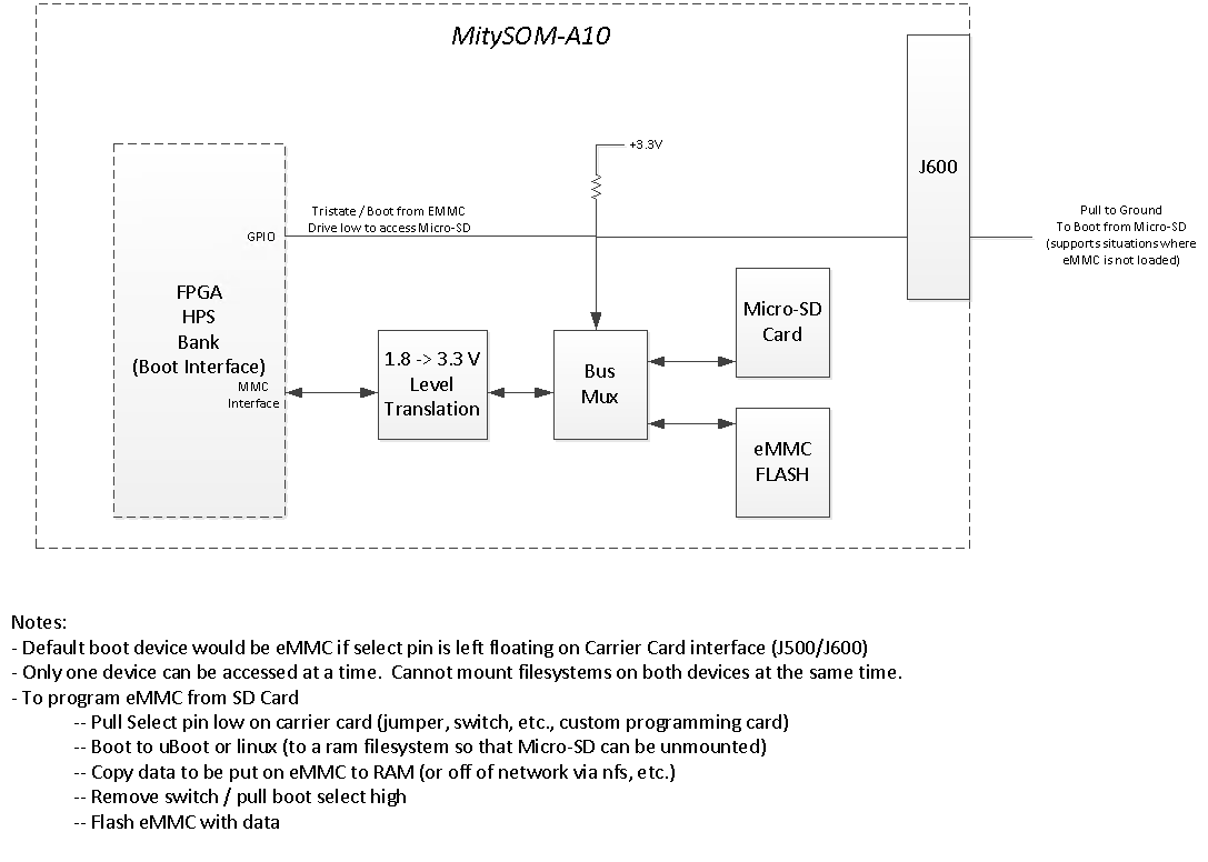
Go to top

