AM57XX/FPGA Communication
Register / Memory Access
There are 2 main mechanisms available for accessing the FPGA from the AM57XX process: the General Purpose Memory Controller (GPMC) 16-bit bus interface, or the PCI-express (PCIe) interface.
GPMC 16 bit bus
The AM57XX GPMC is connected to the FPGA, supporting chip select space 0 with 16 data bits connected. The GPMC is used by the uBoot software to configure the Artix-7 FPGA using Parallel Slave select mode. After the FPGA has been configured, users can continue to leverage this bus for general memory-mapped asynchronous bus transactions using address/data multiplexing mode as described in section 15.4 of the AM5728 technical reference manual. The MitySOM-AM57x does not, by default, using the Address/Data (AD) lines above bit 15, so when using the GPMC in this mode, up to 64K words (or 128 K Bytes) of addressable space is available. Currently, the default Linux and uBoot images provided by Critical Link map the base address of chip select 0 to physical address 0x01000000.
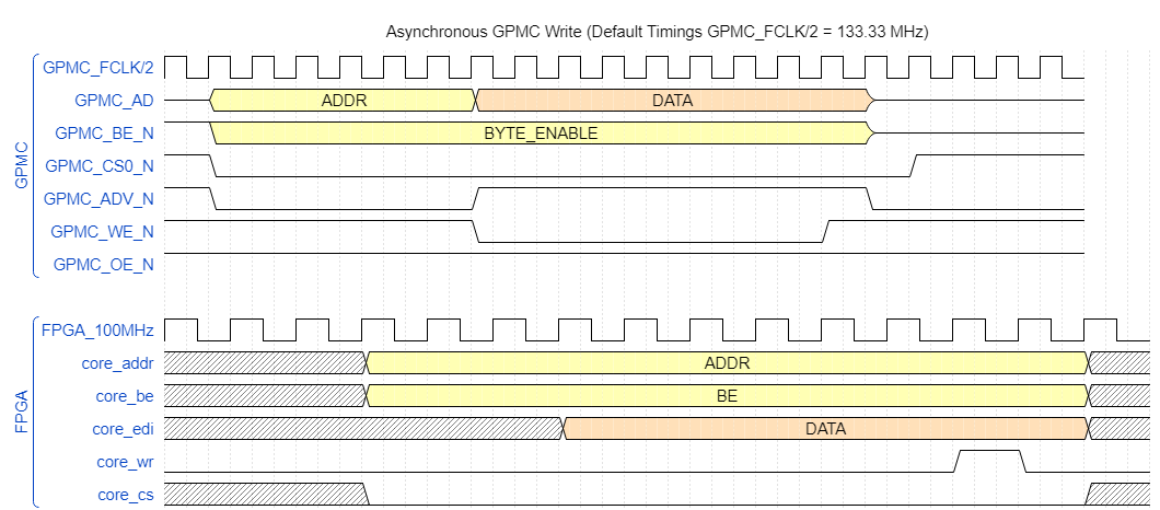
In the reference kernel and device tree provided by Critical Link, the GPMC chip select space is configured with the timings shown in the table and figure below. The timing is configured to support operating with the GPMC_Iface.vhd VHDL module provided by Critical Link to translate memory read and write requests to a local bus format. This design will support the basic IP included in the example projects (for example, GPIO cores, UARTs, etc.) as well as any IP developed for the MityOMAP-L138 product family, allowing for a smooth processor upgrade for users of that platform. It should be noted that the internal GPMC_FCLK is configured, by default, to be 266.66 MHz. In the configuration settings, a clock division of 2 is used to slow the wait states to effectively run on a 133.33 MHz clock timing.
| GPMC REGISTER (CS0) | Address | Value |
|---|---|---|
| CONFIG1 | 0x50000060 | 0x00001210 |
| CONFIG2 | 0x50000064 | 0x00100E00 |
| CONFIG3 | 0x50000068 | 0x00060600 |
| CONFIG4 | 0x5000006C | 0x0E060E06 |
| CONFIG5 | 0x50000070 | 0x000B0F10 |
| CONFIG6 | 0x50000074 | 0x800603C1 |
| CONFIG7 | 0x50000078 | 0x00000F41 |
Currently, the reference project provided by Critical Link uses the GPMC in full asynchronous mode. This is driven by the fact that there is no access to a continuous version the GPMC_CCLK or GPMC_FCLK in order to develop a clock domain with a known phase relationship to the bus data. The GPMC_CCLK signal is a controlled clock in synchronous / burst mode, it is not driven outside of bus access cycles.
The figure below displays an asynchronous write cycle on the GPMC clock / bus domain as well as the output of the Critical Link provided GPMC_Iface.vhd file, which is used for decoding the bus address into 0x80 byte core space regions with an associated chip select strobe (one for each region) and write strobe. The GPMC_Iface.vhd assumes that the reference 100 MHz clock supplied to the MGT clock reference pins is used for internal bus timings.
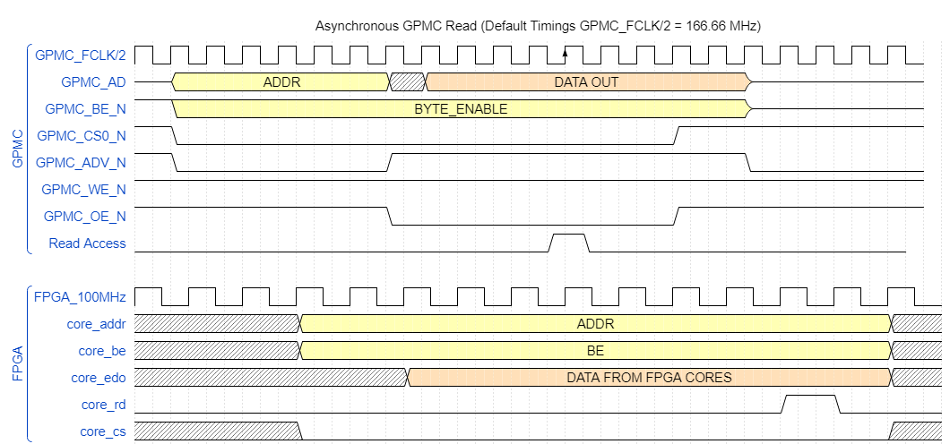
The figure below displays an asynchronous read cycle on the GPMC clock / bus domain as well as the output of the Critical Link provided GPMC_Iface.vhd file, which is used for decoding the bus address into 0x80 byte core space regions with an associated chip select strobe and read strobe. The read strobe can be used to track register reads for the purposes of auto-incrementing pointers or advancing FIFO addresses, etc. The GPMC_IFace.vhd assumes that the reference 100 MHz clock supplied to the MGT clock reference pins is used for internal bus timings.
The timings and mode of the GPMC may be tailored based on your application requirements. The reference design provides a starting point for new designs. It is possible that, even in the asynchronous mode, the GPMC timing may be further optimized. Most of the timing parameters can be configured in the device tree framework when booting from linux.
PCIe
The MitySOM-AM57xx module connects both PCIe lanes between the AM57XX processor and the Artix-7 FPGA. Users may develop whatever interface necessary for their application using this bus.
Xilinx provides several examples and documentation for the 7-series FGPA PCIe end-point control blocks on their 7-Series PCIe Documentation website.
Misc Interfaces
Interrupt Routing
For the GPMC interface, the MitySOM-AM57XX routes FPGA IO pins directly to the SYS_NIRQ1 and SYS_NIRQ2 input pins on the AM57XX processor. The example FPGA project includes a simple FPGA core, called the base_module.vhd, that will support vectorizing up to 16 interrupt sources for each NIRQ line connected to the FPGA. The reference Linux image includes a kernel module, irq-mitysom-am57x-fpga.ko, to route these interrupts to drivers as needed.
If the GPMC interface is not used, these NIRQ pins may be used at the designer's discretion.
For the PCIe interface, it should be possible to use the PCIe Message Signaling Interrupts (MSI) to generate interrupt notifications to attached PCIe drivers.
Video Input Port
TODO
Go to top

