FPGA Overview
This page provides a basic overview of the FPGA interconnectivity on the MitySOM-AM57X System on Module.
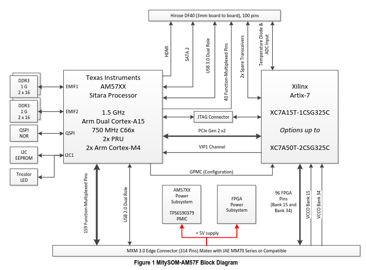
AM57XX Interfaces
There are several direct connect interfaces between the AM57XX processor and the Xilinx FPGA for interprocessor communication.
PCIe
The dual channel PCIe (Gen-1 or Gen-2) link from the AM57XX processor is directly connected to two transceiver lanes on the Artix-7 FPGA in order to facilitate high speed transfers and may be bus mastered by either device.
Note: You must order a MitySOM-AM57XX with the proper Artix Speedgrade of -2 in order to gain the PCIe Gen-2 throughput.
GPMC
The Artix FPGA is configured by the AM572x processor using 16 bit Slave Select over the AM57XX General Purpose Memory controller. After configuration, the GPMC can be used as a general purpose bus interface to the Artix-7. This is similar to the operation of the MityDSP-L138F module architecture.
VIP Port A
In order to facilitate high speed video transfer to the AM57xx processor from custom camera interfaces, a 24 bit Video Input Port (Port A) on the AM57XX processor has been directly connected to the FPGA.
External (off SOM) Interfaces
The remaining FPGA IO interfaces are routed to the SOM external connections, either the MXM card edge connector or the Hirose 100-pin board to board connector.
Bank 34 IO
The MitySOM-AM57x routes 48 IO pins from Bank 34 of the Artix-7 FPGA to the module edge connector. The 48 pins can be used as single ended IO or as up to 24 pair of LVDS IO, and include the SRCC and MRCC dedicated clock pins. The MitySOM-AM57x exposes the VCCO_34 Bank voltage pins to the SOM edge connector in order to support 1.8V, 2.5V or 3.3V single ended IO or LVDS standards. The user must provide the correct reference / bank voltage to this pin while designing their carrier card.
Bank 15 IO
The MitySOM-AM57x also routes 48 IO pins from Bank 15 of the Artix-7 FPGA to the module edge connector. The 48 pins can be used as single ended IO or as up to 24 pair of LVDS IO, and include the SRCC and MRCC dedicated clock pins. The MitySOM-AM57x exposes the VCCO_15 Bank voltage pins to the SOM edge connector in order to support 1.8V, 2.5V or 3.3V single ended IO or LVDS standards. The user must provide the correct reference / bank voltage to this pin while designing their carrier card.
2 Transceiver Interfaces
The MitySOM-AM57x routes 2 pair of Multi-Gigabit Transceivers (MGTs) and one MGT input reference clock to the Hirose board to board connector. If the PCIe block is not needed to communicate with the AM57xx processor in your application, the block may be used to provide external end-point access to the carrier card via this connection. Otherwise, the MGT pair may still be used as general purpose transceiver for user defined serial IO.
XADC Interface
The MitySOM-AM57x routes the VP/VN analog differential input pins of the ADC block to the external connectors in order for customers to take advantage of the 1 Msps 12 bit ADC block. The VREFP reference voltage is connected to an on-board low noise 1.25 V reference.